
4.4: Static fields in inhomogeneous materials
- Page ID
- 25002

Static electric fields in inhomogeneous materials
Many practical problems involve inhomogeneous media where the boundaries may be abrupt, as in most capacitors or motors, or graded, as in many semiconductor or optoelectronic devices. The basic issues are well illustrated by the static cases discussed below. Sections 4.4.1 and 4.4.2 discuss static electric and magnetic fields, respectively, in inhomogeneous media. To simplify the discussion, only media characterized by real scalar values for ε, μ, and σ will be considered, where all three properties can be a function of position.
Static electric fields in all media are governed by the static forms of Faraday’s and Gauss’s laws:
\[\nabla \times \overline{\mathrm{E}}=0\]
\[\nabla \bullet \overline{\mathrm{D}}=\rho_{\mathrm{f}}\]
and by the constitutive relations:
\[\overline{\mathrm{D}}=\varepsilon \overline{\mathrm{E}}=\varepsilon_{\mathrm{o}} \overline{\mathrm{E}}+\overline{\mathrm{P}}\]
\[\overline{\mathrm{J}}=\sigma \overline{\mathrm{E}}\]
A few simple cases illustrate how these laws can be used to characterize inhomogeneous conductors and dielectrics. Perhaps the simplest case is that of a wire or other conducting structure (1) imbedded in a perfectly insulating medium (2) having conductivity σ = 0. Since charge is conserved, the perpendicular components of current must be the same on both sides of the boundary so that \(\mathrm{J}_{1 \perp}=\mathrm{J}_{2 \perp}=0=\mathrm{E}_{2 \perp}\). Therefore all currents in the conducting medium are trapped within it and at the surface must flow parallel to that surface.
Let’s consider next the simple case of an inhomogeneous slab between two parallel perfectly conducting plates spaced L apart in the x direction at a potential difference of Vo volts, where the terminal at x = 0 has the greater voltage. Suppose that the medium has permittivity ε, current density Jo, and inhomogeneous conductivity σ(x), where:
\[\sigma=\sigma_{\mathrm{o}} /\left[1+\frac{\mathrm{x}}{\mathrm{L}}\right]\quad\left[\text { Siemens } \mathrm{m}^{-1}\right]\]
The associated electric field follows from (4.4.4):
\[\overline{\mathrm{E}}=\overline{\mathrm{J}} / \sigma=\hat{x} \frac{\mathrm{J}_{\mathrm{o}}}{\sigma_{\mathrm{o}}}\left(1+\frac{\mathrm{x}}{\mathrm{L}}\right) \quad \left[\mathrm{Vm}^{-1}\right]\]
The free charge density in the medium then follows from (4.4.2) and is:
\[\rho_{\mathrm{f}}=\nabla \bullet \overline{\mathrm{D}}=\left(\varepsilon \mathrm{J}_{\mathrm{o}} / \sigma_{\mathrm{o}}\right)(\partial / \partial \mathrm{x})(1+\mathrm{x} / \mathrm{L})=\varepsilon \mathrm{J}_{\mathrm{o}} / \sigma_{\mathrm{o}} \mathrm{L} \quad\left[\mathrm{Cm}^{-3}\right] \]
Note from the derivative in (4.4.7) that abrupt discontinuities in conductivity generally produce free surface charge ρs at the discontinuity. Although inhomogeneous conductors have a net free charge density throughout the volume, they may or may not also have a net polarization charge density \( \rho_{\mathrm{p}}=-\nabla \bullet \overline{\mathrm{P}}\), which is defined in (2.5.12) and can be deduced from the polarization vector \( \overline{\mathrm{P}}=\overline{\mathrm{D}}-\varepsilon_{\mathrm{o}} \overline{\mathrm{E}}=\left(\varepsilon-\varepsilon_{\mathrm{o}}\right) \overline{\mathrm{E}}\) using (4.4.7):
\[\rho_{\mathrm{p}}=-\nabla \bullet \overline{\mathrm{P}}=-\nabla \bullet\left[\left(\varepsilon-\varepsilon_{\mathrm{o}}\right) \overline{\mathrm{E}}\right]=\left(\varepsilon-\varepsilon_{\mathrm{o}}\right) \mathrm{J}_{\mathrm{o}} / \sigma_{\mathrm{o}} \mathrm{L} \quad \left[\mathrm{Cm}^{-3}\right] \]
Now let’s consider the effects of inhomogeneous permittivity ε(x) in an insulating medium (σ = 0) where:
\[\varepsilon=\varepsilon_{\mathrm{o}}\left(1+\frac{\mathrm{x}}{\mathrm{L}}\right) \]
Since the insulating slab should contain no free charge and the boundaries force \(\overline{\mathrm{D}}\) to be in the x direction, therefore \(\overline{\mathrm{D}}\) cannot be a function of x because \(\nabla \bullet \overline{\mathrm{D}}=\rho_{\mathrm{f}}=0\). But \( \overline{\mathrm{D}}=\varepsilon(\mathrm{x}) \overline{\mathrm{E}}(\mathrm{x})\); therefore the x dependence of \(\overline{\mathrm{E}}\) must cancel that of ε, so:
\[\overline{\mathrm{E}}=\hat{x} \mathrm{E}_{\mathrm{o}} /\left(1+\frac{\mathrm{x}}{\mathrm{L}}\right)\]
Eo is an unknown constant and can be found relative to the applied voltage Vo:
\[\mathrm{V}_{\mathrm{o}}=\int_{0}^{\mathrm{L}} \mathrm{E}_{\mathrm{x}} \mathrm{dx}=\int_{0}^{\mathrm{L}}\left[\mathrm{E}_{\mathrm{o}} /\left(1+\frac{\mathrm{x}}{\mathrm{L}}\right)\right] \mathrm{d} \mathrm{x}=\mathrm{L} \mathrm{E}_{\mathrm{o}} \ln 2\]
Combining (4.4.9–11) leads to a displacement vector \(\overline{\mathrm{D}}\) that is independent of x (boundary conditions mandate continuity of \(\overline{\mathrm{D}}\)), and a non-zero polarization charge density ρp distributed throughout the medium:
\[\overline{\mathrm{D}}=\varepsilon \overline{\mathrm{E}}=\hat{x} \varepsilon_{\mathrm{o}} \mathrm{V}_{\mathrm{o}} /(\mathrm{L} \ln 2)\]
\[\begin{align}
\rho_{\mathrm{p}} &=-\nabla \bullet \overline{\mathrm{P}}=-\nabla \bullet\left(\overline{\mathrm{D}}-\varepsilon_{\mathrm{o}} \overline{\mathrm{E}}\right)=\varepsilon_{\mathrm{o}} \nabla \bullet \overline{\mathrm{E}} \nonumber\\
&=\frac{\varepsilon_{\mathrm{O}} \mathrm{V}_{\mathrm{o}}}{\mathrm{L} \ln 2} \frac{\partial}{\partial \mathrm{x}}(1+\mathrm{x} / \mathrm{L})^{-1}=\frac{-\varepsilon_{\mathrm{o}} \mathrm{V}_{\mathrm{o}}}{(\mathrm{L}+\mathrm{x})^{2} \ln 2}\left[\mathrm{Cm}^{-3}\right]
\end{align}\]
A similar series of computations readily handles the case where both ε and σ are inhomogeneous.
A certain capacitor consists of two parallel conducting plates, one at z = 0 and +V volts and one at z = d and zero volts. They are separated by a dielectric slab of permittivity ε, for which the conductivity is small and different in the two halves of the dielectric, each of which is d/2 thick; σ1 = 3σ2. Assume the interface between σ1 and σ2 is parallel to the capacitor plates and is located at z = 0. What is the free charge density ρf(z) in the dielectric, and what is \(\overline{\mathrm{E}}(\mathrm{z})\) where z is the coordinate perpendicular to the plates?
Solution
Since charge is conserved, \(\overline{\mathrm{J}}_{1}=\overline{\mathrm{J}}_{2}=\sigma_{1} \overline{\mathrm{E}}_{1}=\sigma_{2} \overline{\mathrm{E}}_{2}\), so \( \overline{\mathrm{E}}_{2}=\sigma_{1} \overline{\mathrm{E}}_{1} / \sigma_{2}=3 \overline{\mathrm{E}}_{1}\). But \( \left(\mathrm{E}_{1}+\mathrm{E}_{2}\right) \mathrm{d} / 2=\mathrm{V}\), so \( 4 \mathrm{E}_{1} \mathrm{d} / 2=\mathrm{V}\), and \(\mathrm{E}_{1}=\mathrm{V} / 2 \mathrm{d}\). The surface charge on the lower plate is \(\rho_{\mathrm{s}}(\mathrm{z}=0)=\overline{\mathrm{D}}_{\mathrm{z}=0}=\varepsilon \mathrm{E}_{1}=\varepsilon \mathrm{V} / 2 \mathrm{d}\ \left[\mathrm{C} / \mathrm{m}^{2}\right]\), and ρs on the upper plate is \(-\overline{\mathrm{D}}_{\mathrm{z}=\mathrm{d}}=-\varepsilon \mathrm{E}_{2}=-\varepsilon 3 \mathrm{V} / 2 \mathrm{d}\). Thefree charge at the dielectric interface is \(\rho_{\mathrm{s}}(\mathrm{z}=\mathrm{d} / 2)=\mathrm{D}_{2}-\mathrm{D}_{1}=\varepsilon\left(\mathrm{E}_{2}-\mathrm{E}_{1}\right)=\varepsilon \mathrm{V} / \mathrm{d}\). Charge can accumulate at all three surfaces because the dielectric conducts. The net charge is zero. The electric field between capacitor plates was discussed in Section 3.1.2.
Static magnetic fields in inhomogeneous materials
Static magnetic fields in most media are governed by the static forms of Ampere’s and Gauss’s laws:
\[\nabla \times \overline{\mathrm{H}}=0\]
\[ \nabla \bullet \overline{\mathrm{B}}=0\]
and by the constitutive relations:
\[\overline{\mathrm{B}}=\mu \overline{\mathrm{H}}=\mu_{\mathrm{o}}(\overline{\mathrm{H}}+\overline{\mathrm{M}})\]
One simple case illustrates how these laws characterize inhomogeneous magnetic materials. Consider a magnetic material that is characterized by μ(x) and has an imposed magnetic field \(\overline{\mathrm{B}}\) in the x direction. Since \(\nabla \bullet \overline{\mathrm{B}}=0\) it follows that \(\overline{\mathrm{B}}\) is constant \(\left(\overline{\mathrm{B}}_{\mathrm{o}}\right)\) throughout, and that \(\overline{\mathrm{H}}\) is a function of x:
\[\overline{\mathrm{H}}=\frac{\overline{\mathrm{B}}_{\mathrm{o}}}{\mu(\mathrm{x})}\]
As a result, higher-permeability regions of magnetic materials generally host weaker magnetic fields \(\overline{\mathrm{H}}\), as shown in Section 3.2.2 for the toroidal inductors with gaps. In many magnetic devices μ might vary four to six orders of magnitude, as would \(\overline{\mathrm{H}}\).
Electric and magnetic flux trapping in inhomogeneous systems
Currents generally flow in conductors that control the spatial distribution of \(\overline{\mathrm{J}}\) and electric potential \(\Phi(\overline{\mathrm{r}})\). Similarly, high-permeability materials with μ >> μo can be used to form magnetic circuits that guide \(\overline{\mathrm{B}}\) and control the spatial form of the static curl-free magnetic potential \(\Psi(\bar{r})\).
Faraday’s law says that static electric fields \(\overline{\mathrm{E}}\) are curl-free:
\[\nabla \times \overline{\mathrm{E}}=-\frac{\partial \overline{\mathrm{B}}}{\partial \mathrm{t}}=0 \qquad \qquad \qquad\text{(Faraday’s law)}\]
Since \(\nabla \times \overline{\mathrm{E}}=0 \) in static cases, it follows that:
\[\overline{\mathrm{E}}=-\nabla \Phi\]
where \(\Phi\) is the electric potential [volts] as a function of position in space. But Gauss’s law says \(\nabla \bullet \overline{\mathrm{E}}=\rho / \varepsilon\) in regions where ρ is constant. Therefore \(\nabla \bullet \overline{\mathrm{E}}=-\nabla^{2} \Phi=\rho / \varepsilon \) and:
\[\nabla^{2} \Phi=-\frac{\rho}{\varepsilon} \qquad\qquad\qquad \text { (Laplace's equation) }\]
In static current-free regions of space with constant permeability μ, Ampere’s law (2.1.6) says:
\[\nabla \times \overline{\mathrm{H}}=0\]
and therefore \( \overline{\mathrm{H}}\), like \(\overline{\mathrm{E}} \), can be related to a scalar magnetic potential [Amperes] \(\Psi\):
\[\overline{\mathrm{H}}=-\nabla \Psi\]
Since \( \nabla \bullet \overline{\mathrm{H}}=0\) when μ is independent of position, it follows that \(\nabla \bullet(-\nabla \Psi)=\nabla^{2} \Psi\) and:
\[\nabla^{2} \Psi=0 \qquad \qquad \qquad \text{(Laplace’s equation for magnetic potential) }\]
The perfect parallel between Laplace’s equations (4.4.20) and (4.4.23) for electric and magnetic fields in charge-free regions offers a parallel between current density \(\overline{\mathrm{J}}=\sigma \overline{\mathrm{E}} \ \left[\mathrm{A} / \mathrm{m}^{2}\right]\) and magnetic flux density \( \overline{\mathrm{B}}=\mu \overline{\mathrm{H}}\), and also between conductivity σ and permeability μ as they relate to gradients of electric and magnetic potential, respectively:
\[\nabla^{2} \Phi=0 \qquad \qquad \qquad \nabla^{2} \Psi=0\]
\[\overline{\mathrm{E}}=-\nabla \Phi \qquad \qquad \qquad \overline{\mathrm{H}}=-\nabla \Psi\]
\[\overline{\mathrm{J}}=\sigma \overline{\mathrm{E}}=-\sigma \nabla \Phi\qquad \qquad \qquad \overline{\mathrm{B}}=\mu \overline{\mathrm{H}}=-\mu \nabla \Psi\]
Just as current is confined to flow within wires imbedded in insulating media having σ ≅ 0, so is magnetic flux \(\overline{\mathrm{B}}\) trapped within high-permeability materials imbedded in very low permeability media, as suggested by the discussion in Section 3.2.2 of how magnetic fields are confined within high-permeability toroids.
The boundary condition (2.6.5) that \(\overline{\mathrm{B}}_{\perp} \) is continuous requires that \(\overline{\mathrm{B}}_{\perp} \cong 0 \) at boundaries with media having μ ≅ 0; thus essentially all magnetic flux⎯B is confined within permeable magnetic media having μ >> 0.
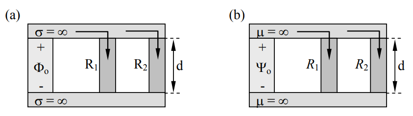
Two parallel examples that help clarify the issues are illustrated in Figure 4.4.1. In Figure 4.4.1(a) a battery connected to perfect conductors apply the same voltage \(\Phi_{\mathrm{o}}\) across two conductors in parallel; Ai, σi, di, and Ii are respectively their cross-sectional area, conductivity, length, and current flow for i = 1,2. The current through each conductor is given by (4.4.26) and:
\[\mathrm{I}_{\mathrm{i}}=\mathrm{J}_{\mathrm{i}} \mathrm{A}_{\mathrm{i}}=\sigma_{1} \nabla \Phi_{\mathrm{i}} \mathrm{A}=\sigma_{\mathrm{l}} \Phi_{\mathrm{o}} \mathrm{A}_{\mathrm{i}} / \mathrm{d}_{\mathrm{i}}=\Phi_{\mathrm{o}} / \mathrm{R}_{\mathrm{i}}\]
where:
\[\mathrm{R}_{\mathrm{i}}=\mathrm{d}_{\mathrm{i}} / \sigma_{\mathrm{i}} \mathrm{A}_{\mathrm{i}} \ [\text { ohms }]\]
is the resistance of conductor i, and I = V/R is Ohm’s law.
For the magnetic circuit of Figure 4.4.1(b) a parallel set of relations is obtained, where the total magnetic flux Λ = BA [Webers] through a cross-section of area A is analogous to current I = JA. The magnetic flux Λ through each magnetic branch is given by (4.4.26) so that:
\[\Lambda_{\mathrm{i}}=\mathrm{B}_{\mathrm{i}} \mathrm{A}_{\mathrm{i}}=\mu_{\mathrm{i}} \nabla \Psi_{\mathrm{i}} \mathrm{A}_{\mathrm{i}}=\mu_{\mathrm{i}} \Psi_{\mathrm{o}} \mathrm{A}_{\mathrm{i}} / \mathrm{d}_{\mathrm{i}}=\Psi_{\mathrm{o}} / R_{\mathrm{i}}\]
where:
\[R_{\mathrm{i}}=\mathrm{d}_{\mathrm{i}} / \mu_{\mathrm{i}} \mathrm{A}\]
is the magnetic reluctance of branch i, analogous to the resistance of a conductive branch.
Because of the parallel between current I and magnetic flux Λ, they divide similarly between alternative parallel paths. That is, the total current is:
\[\mathrm{I}_{\mathrm{o}}=\mathrm{I}_{1}+\mathrm{I}_{2}=\Phi_{0}\left(\mathrm{R}_{1}+\mathrm{R}_{2}\right) / \mathrm{R}_{1} \mathrm{R}_{2}\]
The value of \(\Phi_{\mathrm{o}}\) found from (4.4.31) leads directly to the current-divider equation:
\[\mathrm{I}_{1}=\Phi_{\mathrm{o}} / \mathrm{R}_{1}=\mathrm{I}_{\mathrm{o}} \mathrm{R}_{2} /\left(\mathrm{R}_{1}+\mathrm{R}_{2}\right)\]
So, if R2 = ∞, all Io flows through R1; R2 = 0 implies no current flows through R1; and R2 = R1 implies half flows through each branch. The corresponding equations for total magnetic flux and flux division in magnetic circuits are:
\[\Lambda_{\mathrm{o}}=\Lambda_{1}+\Lambda_{2}=\Psi_{0}\left(R_{1}+R_{2}\right) / R_{1} R_{2}\]
\[\Lambda_{1}=\Psi_{\mathrm{o}} / R_{1}=\Lambda_{\mathrm{o}} R_{2} /\left(R_{1}+R_{2}\right)\]
Although the conductivity of insulators surrounding wires is generally over ten orders of magnitude smaller than that of the wires, the same is not true for the permeability surrounding high-μ materials, so there generally is some small amount of flux leakage from such media; the trapping is not perfect. In this case \(\overline{\mathrm{H}}\) outside the high-μ material is nearly perpendicular to its surface, as shown in (2.6.13).
The magnetic circuit of Figure 4.4.1(b) is driven by a wire that carries 3 amperes and is wrapped 50 times around the leftmost vertical member in a clockwise direction as seen from the top. That member has infinite permeability (μ = ∞), as do the top and bottom members. If the rightmost member is missing, what is the magnetic field \(\overline{\mathrm{H}}\) in the vertical member R1, for which the length is d and μ >> μo? If both R1 and R2 are in place and identical, what then are \(\overline{\mathrm{H}}_{1}\) and \(\overline{\mathrm{H}}_{2}\)? If R2 is removed and R1 consists of two long thin bars in series having lengths da and db, crosssectional areas Aa and Ab, and permeabilities μa and μb, respectively, what then are \(\overline{\mathrm{H}}_{\mathrm{a}} \) and \( \overline{\mathrm{H}}_{\mathrm{b}}\)?
Solution
For this static problem Ampere’s law (4.1.2) becomes
\[\oint_{\mathrm{C}} \overline{\mathrm{H}} \bullet \mathrm{d} \overline{\mathrm{s}}=\oiint_{\mathrm{A}} \mathrm{\overline{J}} \bullet \hat{\mathrm{n}} \mathrm{d} \mathrm{a}=\mathrm{N}\mathrm{I}=50 \times 3=150[\mathrm{A}]=\mathrm{Hd} \nonumber . \]
Therefore \( \overline{\mathrm{H}}=\hat{\mathrm{z}} 150 / \mathrm{d} \ \left[\mathrm{A} \mathrm{m}^{-1}\right]\), where \(\hat{z}\) and \(\overline{\mathrm{H}}\) are upward due to the right-hand rule associated with Ampere’s law. If R2 is added, both the integrals of \(\overline{\mathrm{H}}\) through the two branches must still equal NI, so \(\overline{\mathrm{H}}\) remains \(\hat{z}\) 150/d [A m-1] in both branches. For the series case the integral of \(\overline{\mathrm{H}}\) yields Hada + Hbdb = NI. Because the magnetic flux is trapped within this branch, it is constant: μaHaAa = BaAa = BbAb = μbHbAb. Therefore Hb = Ha(μaAa/μbAb) and Ha[da + db(μaAa/μbAb)] = NI, so \(\overline{\mathrm{H}}_{\mathrm{a}}=\hat{z} \mathrm{NI} /\left[\mathrm{d}_{\mathrm{a}}+\mathrm{d}_{\mathrm{b}}\left(\mu_{\mathrm{a}} \mathrm{A}_{\mathrm{a}} / \mu_{\mathrm{b}} \mathrm{A}_{\mathrm{b}}\right)\right]\ \left[\mathrm{A} \mathrm{m}^{-1}\right]\).