
8.1: Propagation and reflection of transient signals on TEM transmission lines
- Page ID
- 25021

Lossless transmission lines
The speed of computation and signal processing is limited by the time required for charges to move within and between devices, and by the time required for signals to propagate between elements. If the devices partially reflect incoming signals there can be additional delays while the resulting reverberations fade. Finally, signals may distort as they propagate, smearing pulse shapes and arrival times. These three sources of delay, i.e., propagation plus reverberation, device response times, and signal distortion are discussed in Sections 8.1, 8.2, and 8.3, respectively. These same issues apply to any system combining transmission lines and circuits, such as integrated analog or digital circuits, printed circuit boards, interconnections between circuits or antennas, and electrical power lines.
Transmission lines are usually paired parallel conductors that convey signals between devices. They are fundamental to every electronic system, from integrated circuits to large systems. Section 7.1.2 derived from Maxwell’s equations the behavior of transverse electromagnetic (TEM) waves propagating between parallel plate conductors, and Section 7.1.3 showed that the same equations also govern any structure, even a dissipative one, for which the cross-section is constant along its length and that has at least two perfectly conducting elements between which the exciting voltage is applied. Using differential RLC circuit elements, this section below derives the same transmission-line behavior in a form that can readily be extended to transmission lines with resistive wires, as discussed later in Section 8.3.1. Since resistive wires introduce longitudinal electric fields, such lines are no longer pure TEM lines.
Equations (7.1.10) and (7.1.11) characterized the voltage v(t,z) and current i(t,z) on TEM structures with inductance L [H m-1] and capacitance C [F m-1] as:
\[\mathrm{dv} / \mathrm{dz}=-\mathrm{L} \mathrm{di} / \mathrm{dt}\]
\[\mathrm{di} / \mathrm{dz}=-\mathrm{Cdv} / \mathrm{dt}\]
These expressions were combined to yield the wave equation (7.1.14) for lossless TEM lines:
\[\left(\mathrm{d}^{2} / \mathrm{d} \mathrm{z}^{2}-\mathrm{L} \mathrm{C} \mathrm{d}^{2} / \mathrm{dt}^{2}\right) \mathrm{v}(\mathrm{z}, \mathrm{t})=0 \qquad\qquad\qquad \text { (TEM wave equation) }\]
One general solution to this wave equation is (7.1.16):
\[\mathrm{v}(\mathrm{z}, \mathrm{t})=\mathrm{v}_{+}(\mathrm{z}-\mathrm{ct})+\mathrm{v}_{-}(\mathrm{z}+\mathrm{ct}) \qquad \qquad \qquad \text{(TEM voltage) }\]
which corresponds to the superposition of forward and backward propagating waves moving at velocity \(\mathrm{c}=(\mathrm{LC})^{-0.5}=(\mu \varepsilon)^{-0.5}\). The current i(t,z) corresponding to (8.1.4) follows from substitution of (8.1.4) into (8.1.1) or (8.1.2), and differentiation followed by integration:
\[\mathrm{i}(\mathrm{z}, \mathrm{t})=\mathrm{Y}_{\mathrm{o}}\left[\mathrm{v}_{+}(\mathrm{z}-\mathrm{ct})-\mathrm{v}_{-}(\mathrm{z}+\mathrm{ct})\right] \qquad \qquad \qquad \text{(TEM current)}\]
Yo is the characteristic admittance of the line, and the reciprocal of the characteristic impedance Zo:
\[\mathrm{Z}_{\mathrm{o}}=\mathrm{Y}_{\mathrm{o}}^{-1}=(\mathrm{L} / \mathrm{C})^{0.5} \ [\mathrm{Ohms}] \qquad \qquad \qquad \text { (characteristic impedance of lossless TEM line) }\]
The value of Yo follows directly from the steps above.
A more intuitive way to derive these equations utilizes an equivalent distributed circuit for the transmission line composed of an infinite number of differential elements with series inductance and parallel capacitance, as illustrated in Figure 8.1.1(a). This model is easily extended to non-TEM lines with resistive wires.
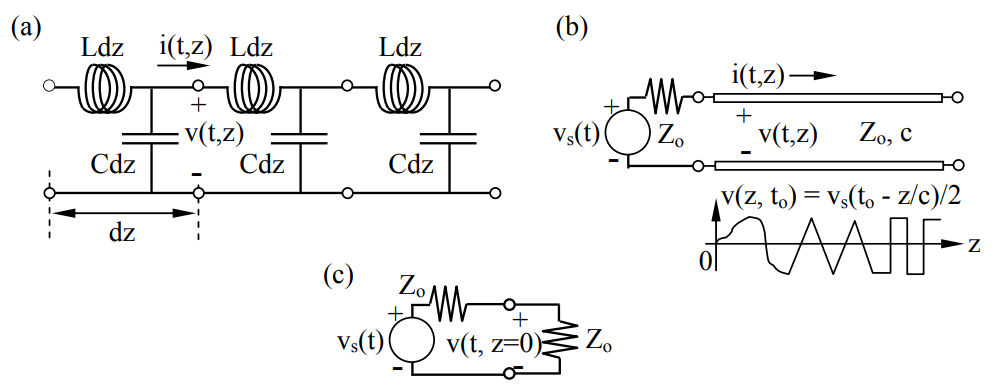
The inductance L [Henries m-1] of the two conductors arises from the magnetic energy stored per meter of length, and produces a voltage drop dv across each incremental length dz of wire which is proportional to the time derivative of current through it40:
\[\mathrm{d} \mathrm{v}=-\mathrm{L} \mathrm{dz}(\mathrm{di} / \mathrm{dt})\]
40 An alternate equivalent circuit would have a second inductor in the lower branch equivalent to that in the upper branch; both would have value Ldz/2, and v(t,z) and i(t,z) would remain the same.
Any current increase di across the distance dz, defined as di = i(t, z+dz) - i(t,z), would be supplied from charge stored in C [F m-1]:
\[\mathrm{di}=-\mathrm{Cdz}(\mathrm{dv} / \mathrm{dt})\]
These two equations for dv and di are equivalent to (8.1.1) and (8.1.2), respectively, and lead to the same wave equation and general solutions derived in Section 7.1.2 and summarized above, where arbitrary waveforms propagate down TEM lines in both directions and superimpose to produce the total v(z,t) and i(t,z).
Two equivalent solutions exist for this wave equation: (8.1.4) and (8.1.9):
\[\mathrm{v(z, t)=f_{+}(t-z / c)+f_{-}(t+z / c)}\]
The validity of (8.1.9) is easily shown by substitution into the wave equation (8.1.3), where again c = (LC)-0.5. This alternate form is useful when relating line signals to sources or loads for which z is constant, as illustrated below. The first form (8.1.4) in terms of (z - ct) is more convenient when t is constant and z varies.
Waves can be launched on TEM lines as suggested in Figure 8.1.1(b). The line is driven by the Thevenin equivalent source vs(t) in series with the source resistance Zo, which is matched to the transmission line in this case. Equations (8.1.4) and (8.1.5) say that if there is no negative traveling wave, then the ratio of the voltage to current for the forward wave on the line must equal Zo = Yo-1. The equivalent circuit for this TEM line is therefore simply a resistor of value Zo, as suggested in Figure 8.1.1(c). If the source resistance is also Zo, then only half the source voltage vs(t) appears across the TEM line terminals at z = 0. Therefore the voltages at the left terminals (z = 0) and on the line v(t,z) are:
\[\mathrm{v}(\mathrm{t}, \mathrm{z}=0)=\mathrm{v}_{\mathrm{s}}(\mathrm{t}) / 2=\mathrm{v}_{+}(\mathrm{t}, \mathrm{z}=0)\]
\[\mathrm{v(t, z)=v_{+}(t-z / c)=v_{s}(t-z / c) / 2} \qquad \qquad \qquad \text{(transmitted signal)}\]
where we have used the solution form of (8.1.9). The propagating wave in Figure 8.1.1(b) has half the amplitude of the Thevenin source vs(t) because the source was matched to the line so as to maximize the power transmitted from the given voltage vs(t). Note that (8.1.11) is the same as (8.1.10) except that z/c was subtracted from each. Equality is preserved if all arguments in an equation are shifted the same amount.
If the Thevenin source resistance were R, then the voltage-divider equation would yield the terminal and propagating voltage v(t,z):
\[\mathrm{v(t, z)=v_{s}(t-z / c)\left[Z_{o} /\left(R+Z_{o}\right)\right]}\]
This more general expression reduces to (8.1.10) when R = Zo and z = 0.
Example \(\PageIndex{A}\)
A certain integrated circuit with μ = μo propagates signals at velocity c/2, and its TEM wires exhibit Zo = 100 ohms. What are ε, L, and C for these TEM lines?
Solution
\(\mathrm{c=\left(\mu_{0} \varepsilon_{0}\right)^{-0.5}}\), and \(\mathrm{v}=\mathrm{c} / 2=\left(\mu_{\mathrm{o}} \varepsilon\right)^{-0.5}\); so ε = 4εo. Since v = (LC)-0.5 and \(Z_{0}=(\mathrm{L} / \mathrm{C})^{0.5}\), \(\mathrm{L}=\mathrm{Z}_{\mathrm{o}} / \mathrm{v}=200 / \mathrm{c}=6.67 \times 10^{-7} \ [\mathrm{Hy}]\), and \(\mathrm{C}=1 / \mathrm{vZ}_{0}=1 / 200 \mathrm{c}=1.67 \times 10^{-11}\ [\mathrm{F}]\).
Reflections at transmission line junctions
If a transmission line connecting a source to a load is sufficiently short, then the effects of the line on reflections can be modeled by simply replacing it with a small lumped capacitor across the source terminals representing the capacitance between the wires, and a resistor in series with an inductor and the load, representing the resistance and inductance of the wires. If, however, the line length D is such that the propagation time \(\tau_{\text { line }}=\mathrm{D} / \mathrm{c}\) is a non-trivial fraction of the shortest time constant of the load \(\tau_{\text { load}}\), then we should use transmission line models governed by the wave equation (e.g., 8.1.3). That is, the TEM wave equation should be used unless the line length D is:
\[\mathrm{D} \ll \mathrm{c} \tau_{\text{ load}}\]
For larger values of D the propagation delays become important and a transmission line model must be used, as explained in Section 8.1.1. Section 8.1.1 also explained how signals are launched and propagate on TEM lines, and how the Thevenin equivalent circuit (8.1.6) for a passive transmission line as seen by the source is simply a resistor Zo = (L/C)0.5. This characteristic impedance Zo of the transmission line is the ratio of the forward voltage v+(t,z) to the associated current i+(z,t). TEM signals are partially transmitted and partially reflected at each junction they encounter, where these junctions may be the intended load or simply places where the impedance Zo of the transmission line changes. Sometimes multiple transmission lines meet at such junctions.
Section 7.2.2 (7.2.7) derived the reflection coefficient \(\Gamma\) for an arbitrary TEM wave v+(t,z) reflected by a load resistance R at z, where the normalized impedance of the load is Rn = R/Zo:
\[\mathrm{v}_{-}(\mathrm{t}, \mathrm{z})=\Gamma \mathrm{v}_{+}(\mathrm{t}, \mathrm{z})\]
\[\Gamma=\left(\mathrm{R}_{\mathrm{n}}-1\right) /\left(\mathrm{R}_{\mathrm{n}}+1\right)\]
\[\mathrm{R_{n} \equiv R / Z_{0}}\]
It is important to distinguish the difference between \(\Gamma\) for purely resistive loads, which is real, and \(\underline{\Gamma}(\omega)\), which is complex and applies to any complex load impedance \(\underline{\mathrm{Z}}_{\mathrm{L}}\). Here R and \(\Gamma\) are real.
Consider the example illustrated in Figure 8.1.2(a), where a TEM line is characterized by impedance Zo and phase velocity c. The line is D meters long, open circuit at the right-hand end, and driven by a unit-step41 voltage u(t). The equivalent circuit at the source end of the line is illustrated in (b), which is simply a voltage divider that places vs(t)/2 volts across the line. But the voltage across the line equals the sum of the forward and backward moving waves, where a passive line at rest has no backward wave. Therefore the forward wave here at z = 0+ is simply u(t)/2, and the result is a voltage of 0.5 volts that moves down the line at velocity c, as illustrated in Figure 8.1.2(c) for t = to. The associated current i(z, t) is plotted in (d) for t = to, and is proportional to the voltage.
41 We use the notation u(t) to represent a unit-step function that is zero for t < 0, and unity for t ≥ 0. A unit impulse is represented by δ(t), which is zero for all |t| > ε in the limit where ε → 0, and the integral of δ(t) ≡ 0. \(\int \delta(\mathrm{t}) \mathrm{dt}=\mathrm{u}(\mathrm{t})\).
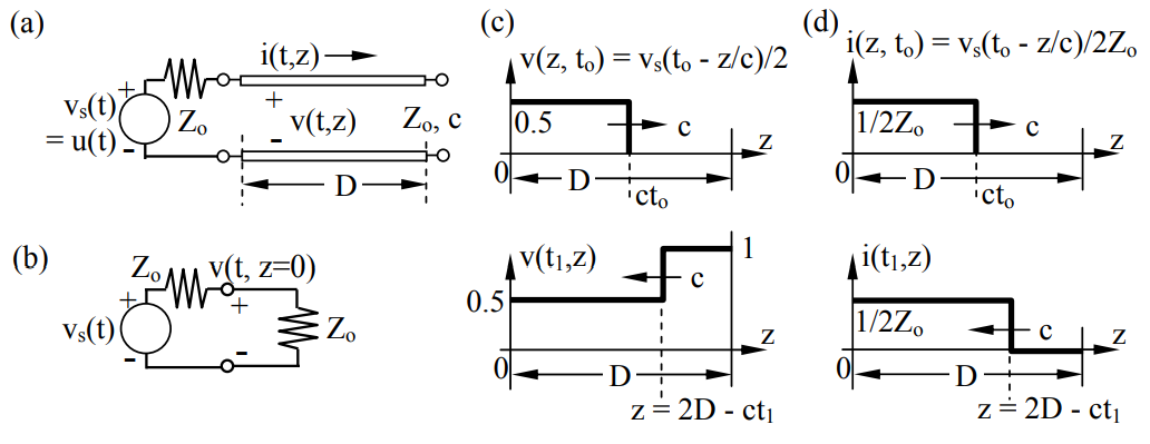
Once the transient reaches the right-hand end, boundary conditions must again be satisfied, so there is a reflected voltage wave having \(\mathrm{v_{-}(t, z=D)=\Gamma v_{+}(t, z=D)}\), where \(\Gamma\) = +1, as given by (8.1.15) for Rn → ∞. The total voltage on the line (8.1.9) is the sum of the forward and backward waves, each of value 0.5 volts, as illustrated in Figure 8.1.2(c) for t = t1 > D/c. At t1 the reflected voltage step is propagating leftward toward the source. The current at t = t1 is plotted in Figure 8.1.2(d).
Although these voltage and current transients are most easily represented and understood graphically, they can also be derived and represented algebraically. For example, v(t, z=0) = u(t)/2 here, and therefore for t < D/c we have v(t,z) = v+(t - z/c) = u(t - z/c)/2. Note that if we translate an argument on one side of an equation, we must impose the same translation on the other; thus v(t,0)→v(t - z/c) forces u(t,0)→u(t - z/c). Once the wave reflects from the open circuit we have v(z,t) = v+(t - z/c) + v-(t + z/c). At z = D for t < 3D/c the boundary condition at the open circuit requires \(\Gamma\) = +1, so v-(t + D/c) = v+(t - D/c) = u(t - D/c)/2. From v-(t + D/c) we can find the more general expression v-(t + z/c) simply by operating on their arguments: v-(t + z/c) = v-(t + D/c –D/c + z/c) = u(t - 2D/c + z/c). The total voltage for t < 2D/c is the sum of these forward and backward waves: v(t,z) = [u(t - z/c) + u(t - 2D/c + z/c)]/2. The same approach can represent line currents and also more complex examples.
When the reflected wave arrives back at the source, \(\Gamma\) = 0 because this source is matched to the transmission line. In this special case there are no further reflections. Steady state is therefore one volt on the line everywhere, with v+ = v- = 0.5 in perpetuity. The total line current is the difference between the forward and backward wave (8.1.5), as plotted in Figure 8.1.2(d) for t1. The steady-state current is therefore zero. These steady state values correspond to ω → 0 and λ → ∞, so the line is then much shorter than any wavelength of interest and can be considered static. We can easily see that an open-circuit line connected to a voltage source via any impedance at all will eventually assume the same voltage as the source, and the current will be zero, as it is here.
If the line were short-circuited at the right-hand end, then \(\Gamma\) = -1 and the voltage v(z) at t1 would resemble that of the current in Figure 8.1.2(d), with the values 0.5 and 0 volts, while the current i(z) at t1 would resemble that of the voltage in (c), with the values 0.5/Zo and 1/Zo. The steady state values for voltage and current in this short-circuit case are zero and 1/Zo, respectively.
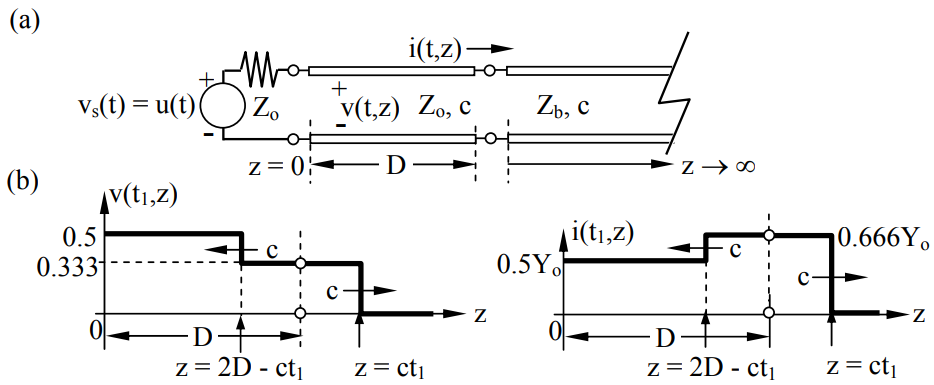
If the first transmission line were connected to a second passive infinite line of impedance Zb, as illustrated in Figure 8.1.3(a), then the same computations would yield v(t,z) and i(t,z) on the first transmission line, where Rn = Zb/Zo. The solution on the second line follows from the boundary conditions: v(t) and i(t) are both continuous across the boundary. The resulting waveforms v(t1,z) and i(t1,z) at time D/c < t1 < 2D/c are plotted in Figure 8.1.3(b) for the case Rn = 0.5, so \(\Gamma\) = - 1/3. In this case the current is increased by the reflection while the voltage is diminished. Independent of the incident waveform, the fraction of the incident power that is reflected is \(\left(\mathrm{v}_{-} / \mathrm{v}_{+}\right)^{2}=\Gamma^{2}\), where the reflection coefficient \(\Gamma\) is given by (8.1.15); the transmitted fraction is \(1-\Gamma^{2}\).
The principal consequence of this reflection phenomenon is that the voltage across a device may not be what was intended if there is an impedance mismatch between the TEM line and the device. This is an issue only when the line is sufficiently long that line delays are non-negligible compared to circuit time constants (8.1.13). The analysis above is for linear resistive loads, but most loads are non-linear or reactive, and their treatment is discussed in Section 8.1.4.
Multiple Reflections and Reverberations
The reflected waves illustrated in Figures 8.1.2 and 8.1.3 eventually impact the source and may be reflected yet again. Since superposition applies if the sources and loads are linear, the contributions from each reflection can be separately determined and then added to yield the total voltage and current. That is, the reflected v-(t,z) will yield its own reflection at the source, and the fate of this reflection can be followed independently of the original forward wave. As usual when analyzing linear circuits, all sources are set to zero when determining the contribution of an independent source such as v-(t,z).
This paradigm is illustrated in Figure 8.1.4, which involves a unit-step current source driving an open-circuited TEM line that is characterized by Zo, c, and length D. Figures 8.1.4(a), (b), and (c) illustrate the circuit, the voltage at t1, and the current at t1, respectively, where t1 = D/2c. The reflection coefficient \(\Gamma\) = 1 (8.1.15) for the open circuit at z = D, so the incident Zo volt step is reflected positively, and the total voltage where they superimpose is 2Zo volts, as illustrated in (d) for t2 = 1.5D/c. The current at this moment is Yo[v+(t - z/c) - v-(t + z/c)], which is zero where the forward and reverse waves overlap, as illustrated in (e). When v-(t + z/c) is reflected from the left-hand end it sees \(\Gamma\) = +1 because, when using superposition, we consider the current source to be zero, corresponding to an open circuit. Thus an additional Zo volts, associated with v+2, adds to v+1 and v-1 to yield a total of 3Zo volts, as illustrated in (f) at t3; the notation v+i refers to the ith forward wave v+. This process continues indefinitely, with the voltage continuing to increase by Zo volts every D/c seconds until something breaks down. Voltage breakdowns are expected when current sources feed open circuits; the finite rate of voltage increase is related to the total capacitance of the TEM line.
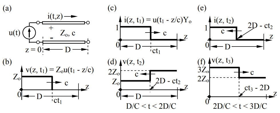
The behavior of the current i(t,z) is interesting too. Figure 8.1.4(c) illustrates how the oneampere current from the current source propagates down the line at velocity c, and (e) shows how the “message” that the line is open-circuited is returned: the current is returning to zero. When this left-moving wave is reflected at the left-hand end the current is again forced to be one ampere by the current source. Thus the current distribution (c) also applies to (f) at t3. This oscillation between one and zero amperes continues indefinitely, much like an unresolved argument between two people, each end of the line forcing the current to satisfy its own boundary conditions while that message propagates back and forth at velocity c.
Example \(\PageIndex{B}\)
A unit step voltage source u(t) with no source resistance drives a short-circuited air-filled TEM line of length D and characteristic impedance Zo = 1 ohm. What current i(t) flows through the short circuit at the end of this TEM line?
Solution
The unit step will propagate down the line, be reflected at the short circuit at z = D where the reflection coefficient \(\Gamma_{\mathrm{D}}\) = -1, and travel back to the voltage source at z = 0, which this transient sees as a short circuit (Δv = 0), also having \(\Gamma_{\mathrm{S}}\) = -1. So, after a round-trip delay of 2D/c, the voltage everywhere on the line is zero, after which a new step voltage travels down the line and superimposes on the first step voltage, thus adding a second step to the current i(t, z=D). This process continues indefinitely as i(t) steps in 1-ampere increments every 2D/C seconds monotonically toward infinity, which is the expected current when a voltage source is shortcircuited. The effect of the line is simply to slow this result as the current and stored magnetic energy on the line build up. More precisely, \(\mathrm{v}(\mathrm{t}, \mathrm{z}=0) \equiv \mathrm{u}(\mathrm{t})=\mathrm{v}_{+1}(\mathrm{t}, \mathrm{z}=0)\). \(\mathrm{v}_{+1}(\mathrm{t}, \mathrm{z}=\mathrm{D})=\mathrm{u}(\mathrm{t}-\mathrm{D} / \mathrm{c})\), so the TEM line presents an equivalent circuit at z = D having Thevenin voltage \(\mathrm{v}_{\mathrm{Th}}=2 \mathrm{v}_{+1}(\mathrm{t}, \mathrm{D})=2 \mathrm{u}(\mathrm{t}-\mathrm{D} / \mathrm{c})\), and Thevenin impedance Zo; this yields \(\mathrm{i}(\mathrm{t})=2 \mathrm{u}(\mathrm{t}-\mathrm{D} / \mathrm{c}) / \mathrm{Z}_{\mathrm{o}}\) for t < 3D/c. Therefore \(\mathrm{v}_{-1}(\mathrm{t} \text { D) }= \mathrm{\Gamma_{D} v_{+1}(t, D)}=-\mathrm{u}(\mathrm{t}-\mathrm{D} / \mathrm{c})\), so \(\mathrm{V}_{+2}(\mathrm{t}, 0)=\Gamma_{\mathrm{S}} \mathrm{v}_{-1}(\mathrm{t}, 0)=\mathrm{u(t-2 D / c)}\). At z = D this second step increases the Thevenin voltage by 2u(t - 3D/c) and increases the current by 2u(t - 3D/c)/Zo, where Zo = 1 ohm. Therefore \(\mathrm{i}(\mathrm{t})=\Sigma_{\mathrm{n}=0}^{\infty} 2 \mathrm{u}(\mathrm{t}-[2 \mathrm{n}+1] \mathrm{D} / \mathrm{c})\).
Reflections by mnemonic or non-linear loads
Most junctions involve mnemonic42 or non-linear loads, where mnemonic loads are capacitors, inductors, or other energy storage devices that have characteristics depending on the past. Nonlinear loads include diodes, transistors, and voltage- or current-dependent capacitors and inductors. In either case the response to arbitrary waveforms cannot be determined by the simple methods described in the previous section. However by simply replacing the transmission line by its equivalent circuit, the voltage and current can generally be easily found, first at the junction and then on the transmission line.
42 Mnemonic means “involving memory”.
The equivalent circuit for an unexcited transmission line is simply a resistor of value Zo because the ratio Δv/Δi for any excitation is always Zo. Determining the voltage across this Zo is generally straightforward even if the source driving the line contains capacitors, inductors, diodes, or similar devices. The forward-propagating wave voltage is simply the terminal voltage, as demonstrated in Figures 8.1.2–4.
The Thevenin equivalent circuit for an energized TEM line has a Thevenin voltage source VTh in series with the Thevenin impedance of the line: ZTh = Zo. Note that the equivalent impedance for a TEM line is exactly Zo, regardless of any loads on the line. The influence of the load at the far end of the line is manifest only in reflected waves that may propagate from it toward the observer, as discussed in the previous section.
The Thevenin equivalent voltage of any linear system is simply its open-circuit voltage. The open-circuit voltage of a transmission line is twice the amplitude of any incident voltage waveform because the reflection coefficient \(\Gamma\) for an open circuit is +1, which doubles the incidence voltage at the junction position zJ:
\[\mathrm{V}_{\mathrm{Th}}\left(\mathrm{t}, \mathrm{z}_{\mathrm{J}}\right)=\mathrm{v}_{+}\left(\mathrm{t}, \mathrm{z}_{\mathrm{J}}\right)+\mathrm{v}_{-}\left(\mathrm{t}, \mathrm{z}_{\mathrm{J}}\right)=2 \mathrm{v}_{+}\left(\mathrm{t}, \mathrm{z}_{\mathrm{J}}\right)\]
The procedure for analyzing a TEM line terminated by any load at z = zJ is then to: 1) solve for the wave v+(t - z/c) traveling toward the load of interest, 2) set \(\mathrm{V}_{\mathrm{Th}}=2 \mathrm{v}_{+}\left(\mathrm{t}-\mathrm{z}_{\mathrm{J}} / \mathrm{c}\right)\) and ZTh = Zo, 3) solve for the terminal voltage v(t, zJ), 4) solve for v-(t,zJ), and 5) find v-(t + z/c), where we define z as increasing toward the load:
\[\mathrm{v}_{-}\left(\mathrm{t}, \mathrm{z}_{\mathrm{J}}\right)=\mathrm{v}\left(\mathrm{t}, \mathrm{z}_{\mathrm{J}}\right)-\mathrm{v}_{+}\left(\mathrm{t}, \mathrm{z}_{\mathrm{J}}\right) \equiv \mathrm{v}_{-}\left(\mathrm{t}+\left[\mathrm{z}_{\mathrm{J}} / \mathrm{c}\right]\right)\]
\[\mathrm{v}_{-}(\mathrm{t}+\mathrm{z} / \mathrm{c})=\mathrm{v}_{-}\left(\mathrm{t}+\left[\left(\mathrm{z}-\mathrm{z}_{\mathrm{J}}\right) / \mathrm{c}\right], \mathrm{z}_{\mathrm{J}}\right) \qquad \qquad \qquad \text{(wave reflected by load)}\]
Equation (8.1.19) says v-(t + z/c) is simply the v-(t, zJ) given by (8.1.18), but delayed by (zJ - z)/c.
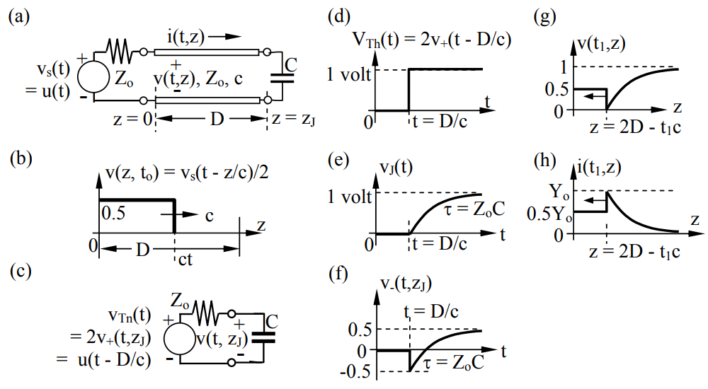
This procedure is best demonstrated by a simple example. Figure 8.1.5(a) illustrates a TEM line driven by a matched unit step voltage source and terminated with a capacitor C. This voltage step, reduced by a factor of two by the voltage divider, propagates toward the capacitor at velocity c, as illustrated in (b). The capacitor sees the Thevenin equivalent circuit illustrated in (c); it consists of Zo in series with a Thevenin voltage source that is twice v+, where v+(t,D) is a 0.5-volt step delayed by the propagation time D/c. Therefore VTh = u(t - D/c), as illustrated in Figure 8.1.5(c) and (d). The solution to the circuit problem of (c) is the junction voltage vJ(t) plotted in (e); it rises exponentially toward its 1-volt asymptote with a time constant \(\mathrm{\tau=Z_{0} C}\) seconds.
To solve for v-(t,zJ) we subtract v+(t,zJ) from vJ(t), as shown in (8.1.18) and illustrated in (f); this then yields v-(t + z/c) using (8.1.19). The total voltage v(t1,z) on the line at time D/c < t1 < 2D/c is plotted in (g) and is the sum of v+(t - z/c), which is 0.5 volts, and v-(t + z/c). The corresponding current i(t1,z) is plotted in (h) and equals Yo times the difference between the forward and reverse voltage waves, as given by (8.1.5). When v-(t,z) arrives at the source, it can be treated just as such waves were treated in Section 8.1.3. In this case the source is matched, so there are no further reflections.
Most digital circuits are non-linear, so this same technique is often used to determine the waveforms on longer TEM lines. Consider the circuit and ramp-pulse voltage source illustrated in Figure 8.1.6(a) and (b).
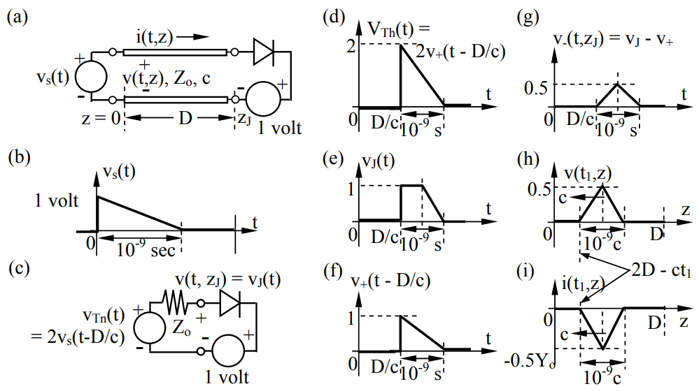
In this case there is no source resistance (an arbitrary choice), so the full value of the source voltage appears across the TEM line. Part (c) shows the equivalent circuit of the transmission line driving the load, which consists of a back-biased diode. The Thevenin voltage VTh(t,zJ) = 2v+(t,zJ) is plotted in (d), the resulting junction voltage vJ(t) is plotted in (e), v+(t,zJ) is plotted in (f), and v-(t,zJ) = vJ(t,zJ) - v+(t,zJ) is plotted in (g). The line voltage and currents at D/c < t1 < 2D/c are plotted in (h) and (i), respectively. Note that these reflected waveforms do not resemble the incident waveform.
Example \(\PageIndex{C}\)
If the circuit illustrated in Figure 8.1.5(a) were terminated by L instead of C, what would be v(t, D), v-(t, D), and v(t,0)?
Solution
Figures 8.1.5(a–d) still apply, except that L replaces C. The one-volt Thevenin step voltage at z = D in series with the Thevenin line impedance Zo yields a voltage v(t, D) across the inductor of u(t - D/c)e-tL/R. Therefore \(\mathrm{v_{-}(t, D)=v(t, D)-v+(t, D)=u(t-\mathrm{D} / \mathrm{c}) \mathrm{e}^{-(\mathrm{t}-\mathrm{D} / \mathrm{c}) \mathrm{L} / \mathrm{R}}-0.5 \mathrm{u}(\mathrm{t}-\mathrm{D} / \mathrm{c})}\) and, since there are no further reflections at the matched load at z = 0, it follows that \(\mathrm{v(t, 0)=0.5 u(t)+u(t-2 D / c) e^{-(t-2 D / c) L R}-0.5 u(t-2 D / c)}\).
Initial conditions and transient creation
Often transmission lines have an initial voltage and current that is interrupted in some way, producing transients. For example, a charged TEM line at rest may have a switch thrown at one end that suddenly connects it to a load, or disconnects it; such a switch could be located in the middle of a line too, either in series or parallel. The solution method has two main steps: 1) determine v+(t,z) and v-(t,z) at t = 0- before the change occurs, and 2) solve for the subsequent behavior of the forward and backward moving waves for the given network configuration.
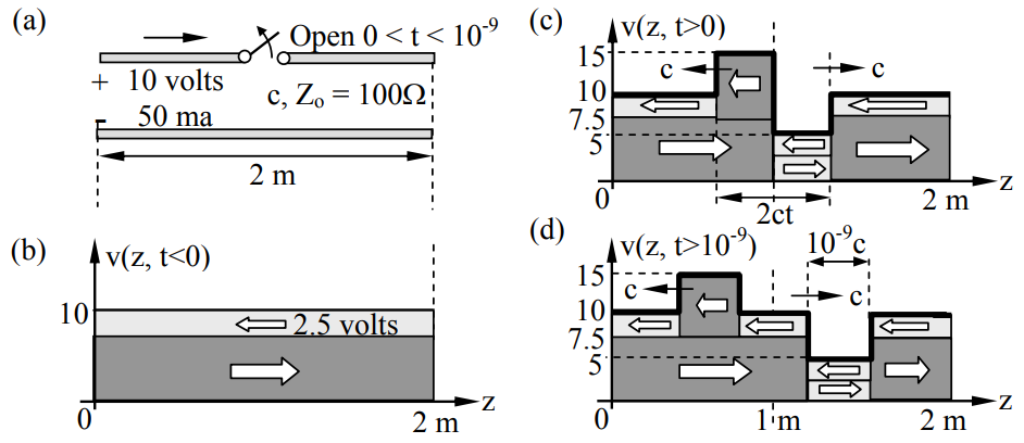
The simple example of Figure 8.1.7 illustrates the method. Assume an air-filled 2-meter long 100-ohm TEM line is feeding a 200-ohm load R with I = 50 milliamperes, when suddenly at t = 0 the line is open-circuited at z = 1 meters for 10-9 seconds, after which it returns to normal. What are the voltage and current on the line as a result of this temporary event?
Using the method suggested above, we first solve for the forward and backward waves prior to t = 0; the current i(t<0, z) is given as I = 50 milliamperes, and the voltage v(t<0, z) = IR is 0.05 × 200 ohms = 10 volts. Note that in steady state Zo does not affect v(t<0, z). We know from (8.1.4) and (8.1.5) that:
\[\mathrm{v(z, t)=v_{+}(z-c t)+v_{-}(z+c t)}\]
\[\mathrm{i}(\mathrm{z}, \mathrm{t})=\mathrm{Y}_{\mathrm{o}}\left[\mathrm{v}_{+}(\mathrm{z}-\mathrm{ct})-\mathrm{v}_{-}(\mathrm{z}+\mathrm{ct})\right]\]
Solving these two equations for v+ and v- yields:
\[\mathrm{v}_{+}(\mathrm{z}-\mathrm{ct})=\left[\mathrm{v}(\mathrm{z}, \mathrm{t})+\mathrm{Z}_{0} \mathrm{i}(\mathrm{z}, \mathrm{t})\right] / 2=[10+5] / 2=7.5 \text { volts }\]
\[\mathrm{v}_{-}(\mathrm{z}+\mathrm{ct})=\left[\mathrm{v}(\mathrm{z}, \mathrm{t})-\mathrm{Z}_{0} \mathrm{i}(\mathrm{z}, \mathrm{t})\right] / 2=[10-5] / 2=2.5 \text { volts }\]
These two voltages are shown in Figure 8.1.7(b), 7.5 volts for the forward wave and 2.5 volts for the reflected wave; this is consistent with the given 50-ma current.
When the switch opens at t = 0 for 10-9 seconds, it momentarily interrupts both v+ and v-, which see an open circuit at the switch and \(\Gamma\) = +1. Therefore in (c) we see 7.5 volts reflected back to the left from the switch, and 2.5 volts reflected back toward the right. At distances closer to the switch than ct [m] we therefore see 15 volts to the left and 5 volts to the right; this zone is propagating outward at velocity c. When the switch closes again, these mid-line reflections cease and the voltages and currents return to normal as the two transient pulses of 15 and 5 volts continue to propagate toward the two ends of the line, as shown in (d), where they might be reflected further.
The currents associated with Figure 8.1.7(d) can easily be surmised using (8.1.21). The effects of the switch are only felt for that brief 10-9-second interval, and otherwise the current on the line is the original 50 ma. In the brief interval when the switch was open the current was forced to zero, and so zero-current pulses of duration 10-9 seconds propagate away from the switch in both directions.
Example \(\PageIndex{D}\)
A 100-ohm air-filled TEM line of length D is feeding 1 ampere to a 50-ohm load when it is momentarily short-circuited in its middle for a time T < D/2c. What are v+(z - ct) and v-(z + ct) prior to the short circuit, and during it?
Solution
For t<0, \(\mathrm{\Gamma=v_{-}(D-c t) / v+(D+c t)=\left(Z_{n}-1\right) /\left(Z_{n}+1\right)=-0.5 / 1.5=-1 / 3}\) where Zn = 50/100. Since the line voltage v(z,t) equals the current i times the load resistance (v = 50 volts), it follows that \(\mathrm{v}_{+}+\mathrm{v}_{-}=2 \mathrm{v}_{+} / 3=50\), and therefore \(\mathrm{v_{+}=v_{+}(z-c t)= 75}\) volts, and v-(z + ct) = -25. During the short circuit the voltage within a distance d = ct of the short is altered. On the source side the short circuit reflects v- = -v+ = -75, so the total voltage (v+ + v-) within ct meters of the short circuit is zero, and on the load side v+ = -v- = 25 is reflected, so the total voltage is again zero. The currents left and right of the short are different, however, because the original v+ ≠ v-, and i+ = v+/Zo. Therefore, on the source side near the short circuit, \(\mathrm{i=\left(v_{+}-\Gamma_{V_{+}}\right) / Z_{0}=2 v_{+} / Z_{0}=2 \times 75 / 50=3 \ [A]}\). On the load side near the short circuit, I = -2×25/50 = -1 [A].