
8.2: Limits Posed by Devices and Wires
- Page ID
- 25022

Introduction to device models
Most devices combine conducting elements with semiconductors, insulators, and air in a complex structure that stores, switches, or transforms energy at rates limited by characteristic time constants governed by Maxwell’s equations and kinematics. For example, in vacuum tubes electrons are boiled into vacuum by a hot negatively charged cathode with small fractions of an electron volt of energy43. Such tubes switch state only so fast as the free electrons can cross the vacuum toward the positively charged anode, and only as fast as permitted by the RL or RC circuit time constants that control the voltages accelerating or retarding the electrons. The same physical limits also apply to most semiconductor devices, as suggested in Section 8.2.4, although sometimes quantum effects introduce non-classical behavior, as illustrated in Section 12.3.1 for laser devices
Design of vacuum tubes for use above ~100 MHz was difficult because high voltages and very small dimensions were required to shorten the electron transit time to fractions of a radio frequency (RF) cycle. The wires connecting the cathode, anode, and any grids to external circuits also contributed inductance that limited speed. Trade-offs were required. For example, as the cathode-anode gap was diminished to shorten electron transit times, the capacitance C between the cathode and anode increased together with delays associated with their RC time constant \(\tau_{\text{ RC}}\). Exactly the same physical issues of gap length, capacitance, and \(\tau_{\text{ RC}}\) arise in most semiconductor devices. The kinematics of electrons in vacuum was discussed in Sections 5.1.2– 3, and the behavior of simple RL and RC circuits was discussed in Section 3.5.1.
43 A thermal energy Eo of one electron volt (≅ 1.6×10⁻¹⁹ [J]) corresponds to a temperature T of ~11,600K, where Eo = kT and k is Boltzmann’s constant: k ≅ 1.38×10⁻²³ [J/o K]. Thus a red-hot cathode at ~1000K would boil off free electrons with thermal energies of ~0.1 e.v.
Semiconductor device models
One simple example illustrates typical sources of lag in semiconductor devices. Both pnp and npn transistors are composed of p-n junctions that contribute device-related delay. Field-effect transistors exhibit related lags. Figures 8.2.1(a) and (b) present a DC p-n junction i-v characteristic and a circuit model that exhibits approximately correct delay characteristics for the case where low-loss metal wires are used for interconnecting devices.
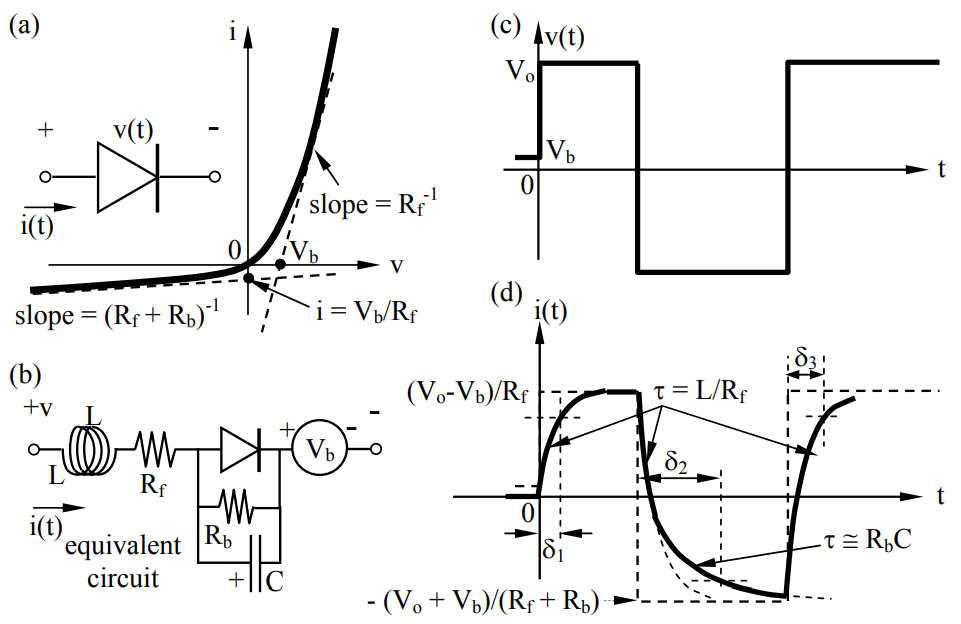
When the ideal diode is forward biased the forward-bias resistance Rf determines the slope of the i-v characteristic. When it is back-biased beyond ~Vb the ideal diode becomes an open circuit so the junction capacitance C becomes important and the back-bias resistance Rf + Rb ≅ Rb determines the slope. C arises because of the charge-free depletion region that exists in backbiased diodes, an explanation of which is given in Section 8.2.4. C decreases as the back-bias voltage increases because the gap width d increases and C ≅ εA/d (3.1.10). The bias voltage Vb in the equivalent circuit is related to the band gap between the valence and conduction bands in the semiconductor, and is ~1 volt for silicon (see Section 8.2.4 for more discussion). The inductance L arises primarily from wires leading externally, and is discussed further in Section 8.2.3 for printed circuits, and estimated in Section 3.3.2 for isolated wires (3.3.17).
Figure 8.2.1(c) represents a typical test voltage across a p-n junction applied as suggested in Figure 8.2.1(a). It begins at that bias voltage v(t) = Vb (~1 volt in silicon), for which the equivalent circuit in Figure 8.2.1(b) conducts no current and the capacitor is discharged. At t = 0+, v(t)→Vo and the current i(t) increases toward (Vo - Vb)/Rf with zero incremental resistance offered by the diode and voltage source, so the time constant \(\tau\) is L/Rf seconds (3.5.10), as illustrated in Figure 8.2.1(d). The capacitor remains uncharged. Section 3.5.1 discusses time constants for simple circuits. As a result of diversion of energy into the inductor, the current i does not reach levels sufficient to trigger the next circuit element until \(\mathrm{t} \cong \delta_{1}\), which is the lag time.
This time constant \(\delta_{1}\) can be easily estimated. For example, a p-n junction might be attached to wires of length D = 0.001 [m] and radius ro = 10-6 [m], and have a forward-biased resistance Rf of ~1 ohm. In this case (3.3.17) yields the wire inductance:
\[\mathrm{L} \cong\left(\mu_{\mathrm{o}} \mathrm{D} / 16 \pi\right) \ln \left(\mathrm{D} / \mathrm{r}_{\mathrm{o}}\right) \cong 1.7 \times 10^{-10} \ [\text {Henries }]\]
Thus \(\delta_{1} \cong \tau=\mathrm{L} / \mathrm{R}=1.7 \times 10^{-10}\) seconds, so the diode might handle a maximum frequency of ~R/2\(\pi\)L Hz, or ~1 GHz. More conservatively the diode might be used at clock frequencies below ~0.2 GHz. Modern computers employ shorter wires and smaller Rf in order to work faster. The circuit model in Figure 8.2.1(b) does not include the capacitance between the wire and the substrate because it is negligibly small here relative to the effects of L.
When the test voltage v(t) then goes negative, the ideal diode in Figure 8.2.1(b) continues to conduct until the current through the inductor decays to zero with the same L/Rf time constant. The current then begins charging C (as the depletion layer is cleared of charge) with a time constant ~RbC that delays the current response for a total of \(\sim \delta_{2}\) seconds. Note that for illustrative purposes the current scale for negative i(t) in (d) has been expanded by a very large factor (Rb/Rf) relative to the scale for positive i(t).
When the test voltage then returns to Vo from its strong negative value, it must first discharge C (re-populate the depletion layer with charge) before the ideal diode in Figure 8.2.1(c) closes, introducing a time constant of ~RfC that we can estimate. If the capacitance C corresponds to a depletion layer of thickness d ≅ 10-7, area A ≅ 10-11 [m2], and permittivity ε ≅ ~10εo, then (3.1.10) yields \(\mathrm{C}=\varepsilon \mathrm{A} / \mathrm{d} \cong 10 \times 8.8 \times 10^{-12} \times 10^{-11} / 10^{-7} \cong 9 \times 10^{-15} \ [\mathrm{F}]\). This yields RfC ≅ 10-14 [s] << L/Rf, so L/Rf would dominate the entire transition, resulting in a total lag of \(\delta_{3} \cong \delta_{1}\) seconds. In reality i(t) in this RLC circuit would ring at ω ≅ (LC)-0.5 radians per second as i(t) and the ringing decay toward the asymptote \(\mathrm{i} \cong\left(\mathrm{V}_{\mathrm{o}}-\mathrm{V}_{\mathrm{b}}\right) / \mathrm{R}_{\mathrm{f}}\).
In most bi-polar transistor circuits using metal wires it is L/Rf that controls the maximum clock speed for the system, which is limited by the slowest junction and the most inductive wires in the entire integrated circuit. In MOS integrated circuits, however, the resistivity of the polysilicon or diffusion layers used for conductors is sufficiently high that the wire inductance is often no longer controlling, as discussed in Section 8.3.1. Wire inductance is most easily reduced by using shorter wider wires, which also reduces wire resistance. Longer paths can be accommodated by using matched TEM lines, as discussed in Section 8.1.
Quasistatic wire models
The lag time for the p-n junction of Figure 8.2.1 was dominated by L/Rf, where L originated in the wires connected to the junction. The effects of depletion layer capacitance C were negligible in comparison for the assumed device parameters. In this section we examine the effects of wire capacitance and cross-section in limiting clock or signal frequencies.
In most integrated circuits the wires are planar and deposited on top of an insulating layer located over a conducting ground plane, as suggested in Figure 8.2.2.
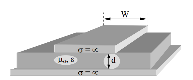
The capacitance and inductance per unit length are C' and L', respectively, which follow from (3.1.10) and (3.2.6) under the assumption that fringing fields are negligible:
\[\mathrm{C}^{\prime}=\varepsilon \mathrm{W} / \mathrm{d} \ \left[\mathrm{F} \mathrm{m}^{-1}\right]\]
\[\mathrm{L}^{\prime}=\mu \mathrm{d} / \mathrm{W} \ \left[\mathrm{H} \mathrm{m}^{-1}\right]\]
\[\mathrm{L}^{\prime} \mathrm{C}^{\prime}=\mu \varepsilon\]
Printed circuit wires with width W ≅ 1 mm and length D ≅ 3 cm printed over dielectrics with thickness d ≅ 1-mm and permittivity ε ≅ 4εo would add capacitance C and inductance L to the connected device, where:
\[\mathrm{C}=\varepsilon \mathrm{WD} / \mathrm{d}=9 \times 8.8 \times 10^{-12} \times 10^{-3} \times 0.03 / 10^{-3}=2.4 \times 10^{-12} \ [\mathrm{F}]\]
\[\mathrm{L}=\mu \mathrm{dD} / \mathrm{W}=1.2 \times 10^{-6} \times 10^{-3} \times 0.03 / 10^{-3}=3.6 \times 10^{-8} \ [\mathrm{H}]\]
These values combine with nominal one-ohm forward-bias resistances of p-n junctions to yield the time constants L/R = 3.6×10⁻⁸ seconds, and RC = 2.4×10⁻¹² seconds. Again the limit is posed by inductance. Such printed circuit boards would be limited to frequencies f ≤ ~1/2\(\pi\)\(\tau\) ≅ 4 MHz.
The numbers cited here are not nearly so important as the notion that interconnections can strongly limit frequencies of operation and circuit utility. The quasistatic analysis above is valid because the physical dimensions here are much smaller than the shortest wavelength (at f = 4 MHz): λ = c/f ≅ 700 meters in air or ~230 meters in a dielectric with ε = 9εo.
We have previously ignored wire resistance in comparison to the nominal one-ohm resistance of forward-biased p-n junctions. If the printed wires above are d =10 microns thick and have the conductivity σ of copper or aluminum, then their resistance is:
\[\mathrm{R}=\mathrm{D} / \mathrm{d} \mathrm{W} \sigma=0.03 /\left(10^{-5} \times 10^{-3} \times 5 \times 10^{7}\right)=0.06 \ [\mathrm{ohms}]\]
Since some semiconductor devices have forward resistances much less than this, wires are sometimes made thicker or wider to compensate. Wider printed wires also have lower inductance [see (8.2.6)]. Width and thickness are particularly important for power supply wires, which often carry large currents.
If (8.2.7) is modified to represent wires on integrated circuits where the dimensions in microns are length D = 100, thickness d = 0.1, and width W = 1, then R = 20 ohms and far exceeds typical forward p-n junction resistances. Limiting D to 20 microns while increasing d to 0.4 and W to 2 microns would lower R to 0.5 ohms. The resistivities of polysilicon and diffusion layers often used for conductors can be 1000 times larger, posing even greater challenges. Clearly wire resistance is another major constraint for IC circuit design as higher operating frequencies are sought.
Example \(\PageIndex{A}\)
A certain integrated circuit device having forward resistance Rf = 0.1 ohms is fed by a polysilicon conductor that is 0.2 microns wide and thick, 2 microns long, and supported 0.1 micron above the ground plane by a dielectric having ε = 10εo. The conductivity of the polysilicon wire is ~5×10⁴ S m-1. What limits the switching time constant \(\tau\) of this device?
Solution
R, L, and C for the conductor can be found from (8.2.7), (8.2.6), and (8.2.5), respectively. \(\mathrm{R}=\mathrm{D} / \mathrm{dW} \sigma=2 \times 10^{-6} /\left[\left(0.2 \times 10^{-7}\right)^{2} 5 \times 10^{4}\right]=1000\),
\[\mathrm{L} \cong \mu \mathrm{dD} / \mathrm{W}=1.26 \times 10^{-6} \times 10^{-7} \times 2 \times 10^{-6} /\left(0.2 \times 10^{-6}\right)=1.26 \times 10^{-12} \quad[\mathrm{Hy}]. \nonumber\]
\[\mathrm{C=\varepsilon W D / d}=8.85 \times 10^{-11} \times 0.2 \times 10^{-6} \times 2 \times 10^{-6} / 10^{-7}=3.54 \times 10^{-16} \ [\mathrm F]. \nonumber\]
\(\mathrm{RC} \cong 3.54 \times 10^{-13} \ [\mathrm{S}]\), \(\mathrm{L} / \mathrm{R}=1.26 \times 10^{-15} \ [\mathrm{S}]\), and \((\mathrm{LC})^{0.5}=2.11 \times 10^{-14}\) [seconds/radian], so RC limits the switching time. If metal substituted for polysilicon, then LC would pose the limit here.
Semiconductors and idealized p-n junctions
Among the most commonly used semiconductors are silicon (Si), germanium (Ge), gallium arsenide (GAs), and indium phosphide (InP). Semiconductors at low temperatures are insulators since all electrons are trapped in the immediate vicinity of their host atoms. The periodic atomic spacing of crystalline semiconductors permits electrons of sufficient energy to propagate freely without scattering, however. Diodes and transistors therefore exhibit conductivities that depend on the applied voltages and resulting electron energy distributions. The response times of these devices are determined by electron kinematics and the response times of the circuits and structures determining voltages and field strengths within the device.
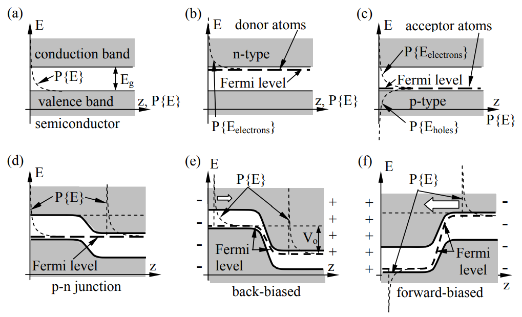
The quantum mechanical explanation of such electron movement invokes the wave nature of electrons, which is governed by the Schroedinger wave equation (not explained here, although it is similar to the electromagnetic wave equation). The consequence is that semiconductors can be characterized by an energy diagram that shows possible electron energy states as a function of position in the z direction, as illustrated in Figure 8.2.3(a). At low temperatures all electrons occupy energy states in the lower valence band, corresponding to bound orbits around atoms. However a second conduction band of possible energy states occupied by freely moving electrons exists at higher energies separated from the valence band by an energy gap Eg that varies with material, but is ~1 e.v. for silicon. For example, a photon with energy hf = Ep > Eg can excite a bound electron in the valence band to a higher energy state in the conduction band where that electron can move freely and conduct electricity. In fact this photo-excitation mechanism is often used in semiconductor photo detectors to measure the intensity of light.
The probability that an unbound electron in thermal equilibrium at temperature T has energy E is governed by the Boltzmann distribution P{E} = e-E/kT/kT, where the Boltzmann constant k = 1.38×10⁻²³ and one electron volt is 1.6×10⁻¹⁹ [J]. Therefore thermal excitation will randomly place a few free electrons in the conduction band since P{E>Eg} > 0. However this provides only extremely limited conductivity because a gap of ~1 e.v. corresponds to a temperature of E/k ≅ 11,600K, much greater than room temperature.44
44 The Fermi level of an undoped semiconductor is midway between the valence and conduction bands, so ~one-half electron volt is actually sufficient to produce excitation, although far more electrons exist in the valence band itself.
To boost the conductivity of semiconductors a small fraction of doping atoms are added that either easily release one electron (called donor atoms), or that easily capture an extra electron (acceptor atoms). These atoms assume energy levels that are just below the conduction band edge (donor atoms) or just above the valence band edge (acceptor atoms), as illustrated in Figure 8.2.3(b) and (c), respectively. These energy gaps are quite small so a significant fraction of the donor and acceptor atoms are typically ionized at room temperature.
The probability that an electron has sufficient energy to leap a gap Ea is the integral of the Boltzmann probability distribution from Ea to E→∞, and Ea is sufficiently small that this integral can approach unity for some dopant atoms. The base energy for the Boltzmann distribution is the Fermi level; electrons fill the available energy levels starting with the lowest and ending with the highest being (on average) at the Fermi level. The Fermi level usually lies very close to the energy level associated with the donor or acceptor atoms, as illustrated in Figure 8.2.3(b–f). Since holes are positively charged, their exponential Boltzmann distribution appears inverted on the energy diagram, as illustrated in (c).
For each ionized donor atom there is an electron in the conduction band contributing to conductivity. For each negatively ionized acceptor atom there is a vacated positively charged “hole” left behind. An adjacent electron can easily jump to this hole, effectively moving the hole location to the space vacated by the jumping electron; in this fashion holes can migrate rapidly and provide nearly the same conductivity as electrons in the conduction band. Semiconductors doped with donor atoms so that free electrons dominate the conductivity are n-type semiconductors (negative carriers dominate), while holes dominate the conductivity of p-type semiconductors doped with acceptors (positive carriers dominate). Some semiconductors are doped to produce both types of carriers. The conductivity of homogeneous semiconductors is proportional to the number of charge carriers, which is controlled primarily by doping density and temperature.
If a p-n junction is short-circuited, the Fermi level is the same throughout as shown in Figure 8.2.3(d). Therefore the tails of the Boltzmann distributions on both sides of the junction are based at the same energy, so there is no net flow of current through the circuit.
When the junction is back-biased by Vo volts as illustrated in (e), the Fermi level is depressed correspondingly. The dominant current comes from the tail of the Boltzmann distribution of electrons in the conduction band of the p-type semiconductor; these few electrons will be pulled to the positive terminal and are indicated by the small white arrow. Some holes thermally created in the n-type valence band may also contribute slightly. Because the carriers come from the high tail of the Boltzmann thermal distribution, the reverse current in a p-n junction is strongly dependent upon temperature and can be used as a thermometer; it is not very dependent upon voltage once the voltage is sufficiently negative. When a p-n junction is backbiased, the electric field pulls back most low-energy free electrons into the n-type semiconductor, and pulls the holes into the p-type semiconductor, leaving a carrier-free layer, called a charge-depletion region, that acts like a capacitor. Larger values of Vo yield larger gaps and smaller capacitance.
When the junction is forward-biased by Vo volts, as illustrated in (f), the charge-free layer disappears and the current flow is dominated by the much greater fraction of electrons excited into the conduction band in the n-type semiconductor because almost all of them will be pulled by the applied electric field across the junction before recombining with a positive ion. This flow of electrons (opposite to current flow) is indicated by the larger white arrow, and is proportional to that fraction of P{E} that lies beyond the small energy gap separating the Fermi level and the lower edge of the conduction band. Holes in the valence band can also contribute significantly to this current. The integral over energy of the exponential probability distribution P{E} above threshold Eg - v is another exponential for 0 < v < Eg, which is proportional to the population of conducting electrons, and which approximates the i(v) relation for a p-n junction illustrated in Figure 8.2.1(a) for v > 0.
Transistors are semiconductor devices configured so that the number of carriers (electrons plus holes) available in a junction to support conductivity is controlled 1) by the number injected into the junction by a p-n interface biased so as to inject the desired number (e.g., as is done in pn-p or n-p-n transistors), or 2) by the carriers present that have not been pulled to one side or trapped by electric fields (e.g., field-effect transistors). In general, small bias currents and voltages can thereby control the current flowing across much larger voltage gaps with power amplification factors of 100 or more. Although the range of device designs is very large, most can be understood semi-classically as suggested above, without the full quantum mechanical descriptions needed for precise characterization.
The response time of p-n junctions and transistors is usually determined by either the RC, RL, or LC time constants that limit the rise and fall times of voltages and currents applied to the device terminals, or by the field relaxation time ε/σ (4.3.3) of the semiconductor material within the device itself. In extremely fast devices the response time sometimes is \(\tau\) ≅ D/v, where D is the junction dimension [m] of interest, and v is the velocity of light t (v = [με]-0.5) or of the transiting electrons (\(\mathrm{v}=\int \mathrm{a} \text{ dt}\), f = ma = eE).
Although these physical models for semiconductor junctions are relatively primitive, they do approximately explain most phenomena.
Example \(\PageIndex{B}\)
What are the approximate temperature dependences of the currents flowing in forward- and reverse-biased p-n junctions?
Solution
If the bias voltage exceeds the gap voltage, and kT is large compared to the energy gap between the donor level and the conduction band, then essentially all donors are ionized and further temperature changes have little effect on forward biased p-n junctions; see Figure 8.2.3(f). The carrier concentration in reverse-biased diodes is proportional to \(\int_{\mathrm{E}_{\mathrm{o}}+\mathrm{Eg}}^{\infty} \mathrm{e}^{-\mathrm{E} / \mathrm{kT}}\) dE , and therefore to T [Figure 8.2.3(e)].