
12.4: Optical detectors, multiplexers, interferometers, and switches
- Page ID
- 25040

Phototubes
Sensitive radio-frequency detectors typically require at least 10-20 Joules per bit of information, which roughly corresponds to thousands of photons of energy hf, where Planck’s constant h = 6.625×10⁻³⁴ Joules Hz-1. This number of photons is sufficiently high that we can ignore most quantum effects and treat the arriving radio signals as traditional waves. In contrast, many optical detectors can detect single photons, although more than five photons are typically used to distinguish each pulse from interference; this requires more energy per bit than is needed at radio wavelengths. The advantage of long-range optical links lies instead in the extremely low losses of optical fibers or, alternatively, in the ability of relatively small mirrors or telescopes to focus energy in extremely small beams so as to achieve much higher gains than can practical radio antennas.
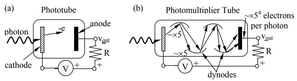
Typical photon detectors include phototubes and semiconductors. A phototube detects photons having energies \(\mathrm{hf}>\Phi\) using the photoelectric effect, where \(\Phi\) is the work function [J] of the metal surface (cathode) that intercepts the photons. Photons with energies above this threshold eject an electron from the cathode with typical probabilities \(\eta\) (called the quantum efficiency) of ~10-30 percent. These ejected electrons are then pulled in vacuum toward a positively charged anode and contribute to the current I through the load resistor R, as illustrated in Figure 12.4.1(a). Although early phototubes ejected electrons from the illuminated surface, it is now common for the metal to be sufficiently thin and transparent that the electrons are emitted from the backside of the metal into vacuum; the metal is evaporated in a thin layer onto the interior surface of the tube’s evacuated glass envelope.
The current I is proportional to the number N of photons incident per second with energies above \(\Phi \):
\[\mathrm{I}=-\eta \mathrm{Ne} \ [\mathrm{A}] \label{12.4.1}\]
The work functions of most metals are ~2-6 electron volts, where the energy of one electron volt (e.v.) is –eV = 1.602×10⁻¹⁹ Joules72. Therefore phototubes do not work well for infrared or longer wavelengths because their energy hf is too small; 2 e.v. corresponds to a wavelength of 0.62 microns and the color red.
72 Note that the energy associated with charge Q moving through potential V is QV Joules, so QV = 1 e.v. = e×1 = 1.602×10⁻¹⁹ Joules.
Because the charge on an electron is small, the currents I are often too small to induce voltages across R (see Figure 12.4.1) that exceed the thermal noise (Johnson noise) of the resistor unless the illumination is bright. Photomultiplier tubes release perhaps 104 electrons per detected photon so as to overcome this noise and permit each detected photon to be unambiguously counted. The structure of a typical photomultiplier tube is illustrated in Figure 12.4.1(b). Each photoelectron emitted by the cathode is accelerated toward the first dynode at ~50-100 volts, and gains energy sufficient to eject perhaps five or more low energy electrons from the dynode that are then accelerated toward the second dynode to be multiplied again. The illustrated tube has four dynodes that, when appropriately charged, each multiply the incident electrons by ~5 to yield ~54 ≅ 625 electrons at the output for each photon detected at the input. Typical tubes have more dynodes and gains of ~104 -107. Such large current pulses generally overwhelm the thermal noise in R, so random electron emissions induced by cosmic rays or thermal effects at the cathode dominate the detector noise. The collecting areas of such tubes can be enhanced with lenses or mirrors.
Photodiodes
Phototubes are generally large (several cubic inches), expensive, and fragile, and therefore semiconductor photodiodes are more commonly used. Photodiodes also respond better to visible and infrared wavelengths and operate at much lower voltages. Figure 12.4.2(a) illustrates the energy diagram for a typical short-circuited p-n junction between p-type and n-type semiconductors, where the vertical axis is electron energy E and the horizontal axis is distance z perpendicular to the planar junction.
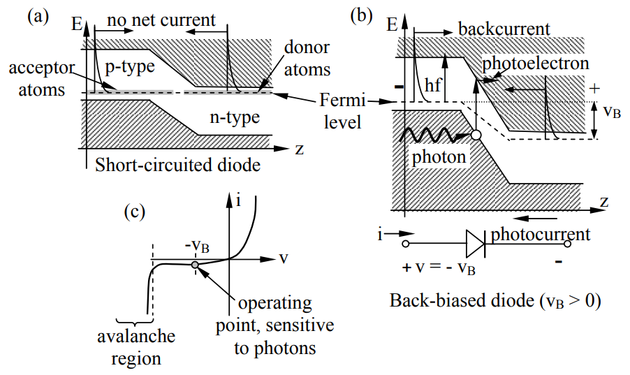
The lower cross-hatched area is the valence band within which electrons are lightly bound to ions, and the upper area is the conduction band within which electrons are free to move in response to electric fields. The band gap between these regions is ~1.12 electron volts (e.v.) for silicon, and ranges from 0.16 e.v. for InSb (indium antimonide to ~7.5 e.v. for BN (boron nitride). In metals there is no such gap and some electrons always reside in the conduction band and are mobile. Additional discussion of p-n junctions appears in Section 8.2.4.
Electrons move freely in the conduction band, but not if they remain in the valence band. Most photons entering the junction region with energy greater than the bandgap between the Fermi level and the lower edge of the conduction band can excite electrons into the conduction band to enhance device conductivity. In semiconductors the Fermi level is that level corresponding to the nominal maximum energy of electrons available for excitation into the conduction band. The local Fermi level is determined by impurities in the semiconductors that create electron donor or acceptor sites; these sites easily release or capture, respectively, a free electron. The Fermi level sits just below the conduction band for n-type semiconductors because donor atoms easily release one of their electrons into the conduction band, as illustrated in Figure 12.4.2(a) and (b). The Fermi level sits just above the valence band for p-type semiconductors because acceptor atoms easily capture an extra electron from bound states in nearby atoms.
If the p-n junction is short-circuited externally, the Fermi level is the same on both halves, as shown in Figure 12.4.2(a). Random thermal excitation produces an exponential Boltzmann distribution in electron energy, as suggested in the figure, the upper tails of which lie in the conduction band on both halves of the junction. When the device is short-circuited these current flows from thermal excitations in the p and n halves of the junction balance, and the external current is zero. If, however, the diode is back-biased by VB volts as illustrated in Figure 12.4.2(b), then the two exponential tails do not balance and a net back-current current flows, as suggested by the I-V characteristic for a p-n junction illustrated in Figure 12.4.2(c). The back current for an un-illuminated photodiode approaches an asymptote determined by VB and the number of thermal electrons excited per second into the conduction band for the p-type semiconductor. When an un-illuminated junction is forward biased, the current increases roughly exponentially.
When a p-n junction is operated as a photodiode, it is back-biased so that every detected photon contributes current flow to the circuit, nearly one electron per photon received. By cooling the photodiode the thermal contribution to diode current can be reduced markedly so that the diode becomes more sensitive to dim light. Cooling is particularly important for photodiodes with the small bandgaps needed for detecting infrared radiation; otherwise the detected infrared signals must be bright so they exceed the detector noise.
If photodiodes are sufficiently back-biased, they can enter the avalanche region illustrated in Figure 12.4.2(c), where an excited electron is accelerated sufficiently as it moves through the semiconductor that it can impact and excite another electron into the conduction band; both electrons can now accelerate and excite even more electrons, exponentially, until they all exit the high-field zone so that further excitations are not possible. In response to a single detected photon such avalanche photodiodes (APD’s) can produce an output pulse of ~104 electrons that stands out sufficiently above the thermal noise that photons can again be counted individually. The number of photons detected per second is proportional to input power, and therefore to the square of the incident electric field strength.
Frequency-multiplexing devices and filters
The major components in fiber-optic communications systems are the fibers themselves and the optoelectronic devices that manipulate the optical signals, such as detectors (discussed in Sections 12.4.1–2), amplifiers and sources (Section 12.3), multiplexers and filters (this section), modulators, mixers, switches, and others (Section 12.4.4). These are assembled to create useful communications, computing, or other systems.
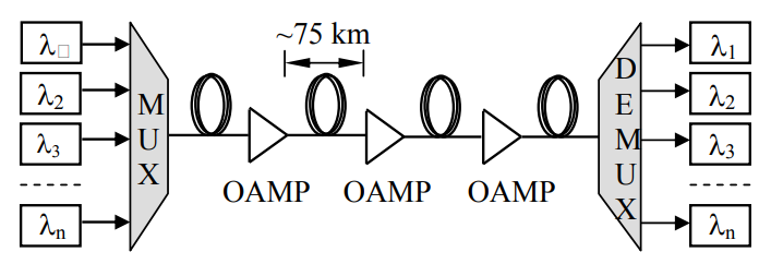
A typical wave-division multiplexed (WDM) amplifier is pictured in Figure 12.4.3; narrowband optical signals of different colors are aggregated at a point of departure and merged onto a single long fiber by a frequency multiplexer (MUX). Along this fiber extremely broadband optical amplifiers (OAMPs) are spaced perhaps 80 km apart to sustain the signal strength. OAMPs today are typically erbium-doped fiber amplifiers (EFDA’s). At the far end the signal is de-multiplexed into its spectral components, which are then directed appropriately along separate optical fibers. Before broadband amplifiers were available, each narrow band had to have separate amplifiers and often separate fibers.
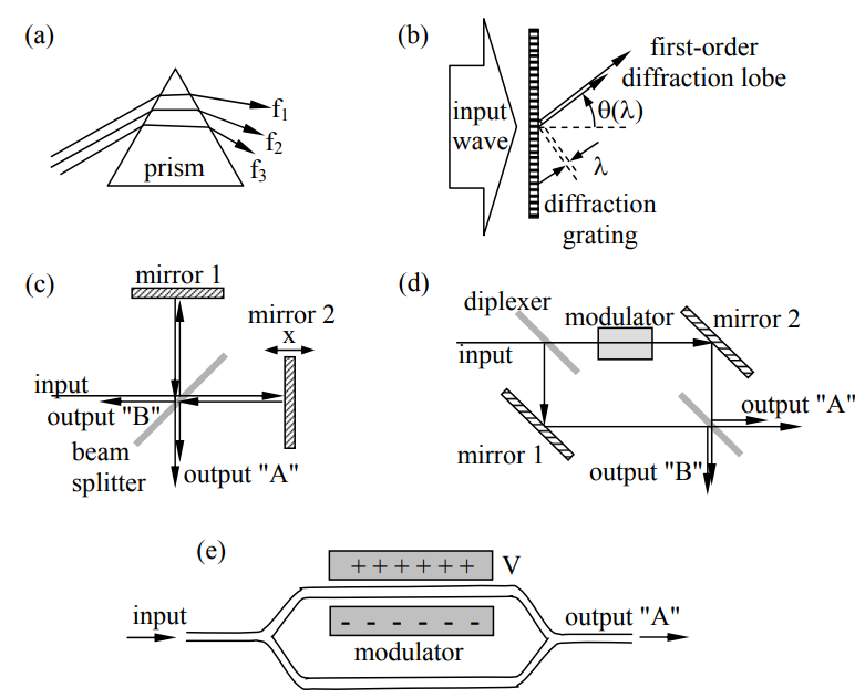
Such multiplexers can be made using prisms or diffraction gratings that refract or diffract different colors at different angles, as suggested in Figure 12.4.4(a) and (b); by reciprocity the same devices can be used either for multiplexing (superimposing multiple frequency bands on one beam) or demultiplexing (separation of a single beam into multiple bands), depending on which end of the device receives the input.
The diffraction grating of Figure 12.4.4(b) is typically illuminated by normally incident uniform plane waves, and consists of closely spaced ruled straight lines where equal-width stripes typically alternate between transmission and reflection or absorption. Alternate stripes sometimes differ only in their phase. Each stripe must be more than λ/2 wide, and λ is more typical. In this case the rays from each transparent stripe 2λ apart will add in phase straight forward (θ = 0) and at \(\theta=\sin ^{-1}(\lambda / 2 \lambda)=30^{\circ}\), exactly analogous to the grating lobes of dipole array antennas (Section 10.4). Since the stripe separation (2λ here) is fixed, as the frequency f = c/λ varies, so does θ, thus directing different frequencies toward different angles of propagation, much like the prism.
Another useful optical device is the Fabry-Perot resonator, which is the optical version of the TEM resonator illustrated in Figure 7.4.3(a) and explained in Section 7.4.3. For example, an optical TEM resonator can be fabricated using parallel mirrors with uniform plane waves trapped between them; the allowed resonator modes have an integral number n of half-wavelengths in the distance L between the parallel conductors:
\[\mathrm{n} \lambda_{\mathrm{n}} / 2=\mathrm{L} \label{12.4.2}\]
Thus the frequency fn of the nth TEM resonance is:
\[\mathrm{f}_{\mathrm{n}}=\mathrm{c} / \lambda_{\mathrm{n}}=\mathrm{nc} / 2 \mathrm{L} \ [\mathrm{Hz}] \label{12.4.3}\]
and the separation between adjacent resonances is c/2L [Hz]. For example, if L is 1.5 mm, then the resonances are separated 3×10⁸/0.003 = 100 GHz.
If the input and output mirrors transmit the same small fraction of the power incident upon them, then the “internal” and external Q’s of this resonator are the same, where the “internal Q” here (QI) is associated with power escaping through the output mirror and the “external Q” (QE) is associated with power escaping through the input mirror. As suggested by the equivalent circuits in Figures 7.4.4–5, there is perfect power transmission through the resonator at resonance when the internal and external Q’s are the same, provided there are no dissipative losses within the resonator itself. The width of the resonance is then found from (7.4.45–6):
\[\Delta \omega=\omega_{\mathrm{o}} / \mathrm{Q}_{\mathrm{L}}=2 \omega_{\mathrm{o}} / \mathrm{Q}_{\mathrm{E}}=2 \mathrm{P}_{\mathrm{E}} / \mathrm{w}_{\mathrm{T}} \label{12.4.4}\]
The loaded QL = QE/2 when QE = QI, and PE [W] is the power escaping through the input mirror when the total energy stored in the resonator is wT [J]. With high reflectivity mirrors and low residual losses the bandwidth of such a resonator can be made almost arbitrarily narrow. At optical frequencies the ratio of cavity length L to wavelength λ is also very large. This increases the ratio of wT to PE proportionally and leads to very high QL and narrow linewidth.
If the medium in a Fabry-Perot interferometer is dispersive, then it can be shown that the spacing between resonances is vg/2L [Hz], or the reciprocal of the round-trip time for a pulse. Thus such a resonator filled with an active medium could amplify a single pulse that rattles back and forth in the resonator producing sharp output pulses with a period 2L/vg. The Fourier transform of this pulse train is a train of impulses in the frequency domain with spacing vg/2L, i.e., representing the set of resonant frequencies for this resonator. The resonant modes of such a mode-locked laser are synchronized, so they can usefully generate pulse trains for subsequent modulation.
What is the ratio of the width Δω of the passband for a Fabry-Perot resonator relative to the spacing ωi+1 - ωi between adjacent resonances? What power transmission coefficient \(\mathrm{T}^{2}=\left|\mathrm{\underline E}_{\mathrm{t}}\right|^{2} \big/\left|\mathrm{\underline E}_{\mathrm{i}}\right|^{2} \) is required for each mirror in order to produce isolated sharp resonances? What is the width Δf [Hz] of each resonance?
Solution
The resonance width Δω and spacing are given by (\ref{12.4.4}) and (\ref{12.4.2}), respectively, so:
\[\Delta \omega /\left(\omega_{\mathrm{i}+1}-\omega_{\mathrm{i}}\right)=\left(2 \mathrm{P}_{\mathrm{E}} / \mathrm{w}_{\mathrm{T}}\right) /(\pi \mathrm{c} / \mathrm{L})=\left[\left(2 \mathrm{P}_{+} \mathrm{T}^{2}\right) /\left(2 \mathrm{LP}_{+} / \mathrm{c}\right)\right](\mathrm{L} / \pi \mathrm{c})=\mathrm{T}^{2} / \pi<\sim 0.3 \nonumber\]
Therefore we require T2 < ~1 so that \(\Delta \omega<\sim 0.3\left(\omega_{i+1}-\omega_{i}\right)\).
\(\Delta \mathrm{f}=\Delta \omega / 2 \pi=\left(\mathrm{T}^{2} / \pi\right)\left(\omega_{\mathrm{i}+1}-\omega_{\mathrm{i}}\right) / 2 \pi=\left(\mathrm{T}^{2} / \pi\right) \mathrm{c} / 2 \mathrm{L}\ [\mathrm{Hz}]\); it approaches zero as T2/L does.
Interferometers
The Michelson interferometer and the Mach-Zehnder interferometer are important devices illustrated in Figure 12.4.4(c) and (d), respectively. In both cases an input optical beam is split by a beam-splitter into two coherent beams that are reflected by mirrors and then recombined coherently in a second beam-splitter to form two output beams. The intensity of each output beam depends on whether its two input components added in-phase or out-of-phase. The beamsplitters are typically dielectric mirrors coated so that half the power is reflected and half transmitted from the front surface; the rear surface might be anti-reflection coated. Half-silvered mirrors can also be used.
As the position x of a Michelson mirror varies, the output power varies sinusoidally from zero, which results when the two beams cancel at the output, to its peak value when the two beams add in phase. Cancellation requires that the two beams have equal strength. It is interesting to ask where the input power goes when output “A” is zero; the figure suggests the answer. The missing power emerges from the other output; the sum of the powers emerging from the two outputs equals the input power, less any dissipative losses. This requirement for power conservation translates into a requirement for a specific phase relationship between the various beams.
Consecutive peaks in output strength occur as the mirror moves λ/2 (typically ~3×10⁻⁷ m); the factor of 1/2 arises because of the round trip taken by the reflected beam. The sinusoidal output power can generally be measured with sufficient accuracy at optical wavelengths to determine relative mirror positions x with accuracies of an angstrom (10-10 m), or tiny fractions thereof; thus the Michelson interferometer is a powerful tool for measuring or comparing wavelengths and distances. Another important application is measurement of optical spectra. Since each optical wavelength λ in the input beam produces an additive sinusoidal contribution to the output power waveform A(x) of period λ/2, the input optical power spectrum is the Fourier transform of A(2x). Because this technique was first used to analyze infrared spectra, it is called Fourier transform infrared spectroscopy (FTIR).
If the two output beams in a Mach-Zehnder interferometer add in phase, the output power is maximized and equals the input power, much like the Michelson interferometer. In either type of interferometer the phase of the optical beam in one arm can be modulated by varying the effective dielectric constant and delay of its propagation medium; certain dielectrics are tunable when biased with large electric fields. In this fashion the output beam power can be modulated by varying the voltage V across the propagation medium, as illustrated in Figure 12.4.4(d) and (e). If the device operates near a transmission null, very little change in refractive index is required to produce a large increase in output power. Such devices can modulate optical power at frequencies of 10 GHz or more.
The Mach-Zehnder interferometer configuration in Figure 12.4.4(e) is widely used for modulators because the waveguides can be integrated on a chip together with other optical components. The output is maximum when the two arms have equal phase delays. When the two merging beams are out of phase the excited waveguide mode is not trapped in the output waveguide but radiates away; the radiated wave corresponds to output B in Figure 12.4.4(d). The same integrated configuration can alternatively be used as a notch filter, eliminating an undesired optical wavelength for which the two arm lengths differ by exactly λ/2, while passing nearby wavelengths.
Optical switches
Optical switches redirect optical beams just as electrical switches redirect currents. One approach is to use MEMS devices that mechanically move mirrors or shutters to redirect the light beams, which usually are narrow, coherent, and laser-produced. Such devices can switch light beams at rates approaching 1 MHz.
Another approach is to direct the light beam at right angles to a dielectric within which ultrasonic acoustic waves (at radio frequencies) are propagating transverse to the light so as to produce a dynamic phase grating through which the light propagates and diffracts. The configuration is that of Figure 12.4.4(b). The acoustic waves compress and decompress the medium in a wavy pattern; the compressed regions have a slightly higher permittivity and therefore a slightly lower velocity of light. By making the dielectric sufficiently thick, the cumulative phase variation of the light passing through the device can be λ/2 or more, thus producing strong diffraction at an angle θ corresponding to the wavelength of light λ and the acoustic wavelength \(\lambda_{\mathrm{a}}\), where \( \theta=\sin ^{-1}\left(\lambda / \lambda_{\mathrm{a}}\right)\) and \(\lambda_{\mathrm{a}} \cong 2 \lambda \). In practice the cumulative phase variation is often much less than λ/2 because of improved simplicity, linearity, and the availability of high input powers that can compensate for the reduced diffractive power efficiency. In this fashion the diffracted beam can be steered among several output ports at rates up to ~1 MHz or more, limited largely by the time it takes the acoustic wave to traverse the diffraction zone. Acoustic velocities in solids are roughly 1000-3000 m/s.
A more important method, however, is the use of Mach-Zehnder interferometers (see Section 12.4.4) to modulate input optical streams, varying their intensity by more than 15 dB at rates up to ~10 GHz, limited by the time it takes the signals modulating the electrical phase length modulator of Figure 12.4.4(e) to propagate across that modulator (e.g. nanoseconds). The detected modulator output signal is the product of the optical and modulator signals. The spectrum of this product contains the convolution of the two input spectra, which exhibits upper and lower sidebands that correspond to the radio frequency signal being communicated.