
2.5: Electric and Magnetic Fields in Media


( \newcommand{\kernel}{\mathrm{null}\,}\)
Maxwell’s equations and media
The great success of Maxwell’s equations lies partly in their simple prediction of electromagnetic waves and their simple characterization of materials in terms of conductivity σ [Siemens m-1], permittivity ε [Farads m-1], and permeability μ [Henries m-1]. In vacuum we find σ = 0, ε = εo, and μ = μo, where εo = 8.8542×10⁻¹² and μo = 4π×10-7. For reference, Maxwell’s equations are:
∇×→E=−∂→B∂t
∇×→H=→J+∂→D∂t
∇∙ˉD=ρ
∇∙→B=0
The electromagnetic properties of most media can be characterized by the constitutive relations:
→D=ϵ→E
→B=μ→H
→J=σ→E
In contrast, the nano-structure of media can be quite complex and requires quantum mechanics for its full explanation. Fortunately, simple classical approximations to atoms and molecules suffice to understand the origins of σ, ε, and μ, as discussed below in that sequence.
Conductivity
Conduction in metals and n-type semiconductors6 involves free electrons moving many atomic diameters before they lose momentum by interacting with atoms or other particles. Acceleration induced by the small applied electric field inside the conductor restores electron velocities to produce an equilibrium current. The total current density →J [A m-2] is proportional to the product of the average electron velocity →v [m s-1] and the number density n [m-3] of free electrons. A related conduction process occurs in ionic liquids, where both negative and positive ions can carry charge long distances
In metals there is approximately one free electron per atom, and in warm n-type semiconductors there is approximately one free electron per donor atom, where the sparse donor atoms are easily ionized thermally. Since, for non-obvious reasons, the average electron velocity ⟨ˉv⟩ is proportional to →E, therefore →J=−en3⟨→v⟩=σ→E, as stated in (2.5.7). As the conductivity σ approaches infinity the electric field inside a conductor approaches zero for any given current density →J.
Warm donor atoms in n-type semiconductors can be easily ionized and contribute electrons to the conduction band where they move freely. Only certain types of impurity atoms function as donors--those that are most easily ionized. As the density of donor atoms approaches zero and as temperature declines, the number of free electrons and the conductivity approach very low values that depend on temperature and any alternative ionization mechanisms that are present.
In p-type semiconductors the added impurity atoms readily trap nearby free electrons to produce a negative ion; this results in a corresponding number of positively ionized semiconductor atoms that act as “holes”. As a result any free electrons typically move only short distances before they are trapped by one of these holes. Moreover, the threshold energy required to move an electron from a neutral atom to an adjacent positive ion is usually less than the available thermal energy, so such transfers occur rapidly, causing the hole to move quickly from place to place over long distances. Thus holes are the dominant charge carriers in p-type semiconductors, whereas electrons dominate in n-type semiconductors.
6 n-type semiconductors (e.g., silicon, germanium, gallium arsenide, indium phosphide, and others) are doped with a tiny percentage of donor atoms that ionize easily at temperatures of interest, releasing mobile electrons into the conduction band of the semiconductor where they can travel freely across the material until they recombine with another ionized donor atom. The conduction band is not a place; it refers instead to an energy and wave state of electrons that enables them to move freely. The conductivity of semiconductors therefore increases with temperature; they become relatively insulating at low temperatures, depending on the ionization potentials of the impurity atoms.
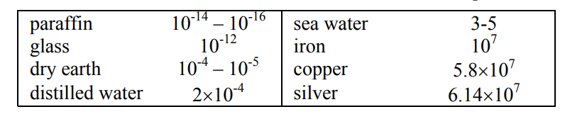
More broadly, semiconductors have a conduction band in which free electrons can propagate long distances; this band is separated by an energy of one or a few electron volts from the valence band in which electrons cannot move. The conduction band is not a location, it is a family of possible electron wave states. When electrons are excited from the valence band to the conduction band by some energetic process, they become free to move in response to electric fields. Semiconductor conductivity is approximately proportional to the number of free electrons or holes produced by the scarce impurity atoms, and therefore to the doping density of those impurity atoms. Easily ionized impurity atoms are the principal mechanism by which electrons enter the conduction band, and impurities that readily trap adjacent electrons are the principal mechanism by which holes enter and move in the valence band. Semiconductors are discussed further in Section 8.2.4. The current leakage processes in insulators vaguely resemble electron and hole conduction in semiconductors, and can include weak surface currents as well as bulk conduction; microscopic flaws can also increase conductivity. The conductivities of typical materials are listed in Table 2.5.1.
Table 2.5.1: Nominal conductivities σ of common materials [Siemens m-1].
In some exotic materials the conductivity is a function of direction and can be represented by the 3×3 matrix ˉˉσ; such materials are not addressed here, but Section 2.5.3 addresses similar issues in the context of permittivity ε.
Some materials exhibit superconductivity, or infinite conductivity. In these materials pairs of electrons become loosely bound magnetically and move as a unit called a Cooper pair. Quantum mechanics prevents these pairs from colliding with the lattice and losing energy. Because the magnetic binding energy for these pairs involves electron spins, it is quite small. Normal conductivity returns above a threshold critical temperature at which the pairs are shaken apart, and it also returns above some threshold critical magnetic field at which the magnetic bonds coupling the electrons break as the electron spins all start to point in the same direction. Materials having critical temperatures above 77K (readily obtained in cryogenic refrigerators) are difficult to achieve. The finite number of such pairs at any temperature and magnetic field limits the current to some maximum value; moreover that current itself produces a magnetic field that can disrupt pairs. Even a few pairs can move so as to reduce electric fields to zero by short circuiting the normal electrons until the maximum current carrying capacity of those pairs is exceeded. If the applied fields have frequency f > 0, then the Cooper pairs behave much like collisionless electrons in a plasma and therefore the applied electric field can penetrate that plasma to its skin depth, as discussed in Section 9.8. Those penetrating electric fields interact with a small number of normal electrons to produce tiny losses in superconductors that increase with frequency.
Permittivity
The permittivity εo of free space is 8.854×10⁻¹² farads/meter, where →D=εo→E. The permittivity ε of any material deviates from εo for free space if applied electric fields induce electric dipoles in the medium; such dipoles alter the applied electric field seen by neighboring atoms. Electric fields generally distort atoms because →E pulls on positively charged nuclei ( f= q→E [N]) and repels the surrounding negatively charged electron clouds. The resulting small offset →d of each atomic nucleus of charge +q relative to the center of its associated electron cloud produces a tiny electric dipole in each atom, as suggested in Figure 2.5.1(a). In addition, most asymmetric molecules are permanently polarized, such as H2O or NH3, and can rotate within fluids or gases to align with an applied field. Whether the dipole moments are induced, or permanent and free to rotate, the result is a complete or partial alignment of dipole moments as suggested in Figure 2.5.1(b).
These polarization charges generally cancel inside the medium, as suggested in Figure 2.5.1(b), but the immobile atomic dipoles on the outside surfaces of the medium are not fully canceled and therefore contribute the surface polarization charge ρsp.
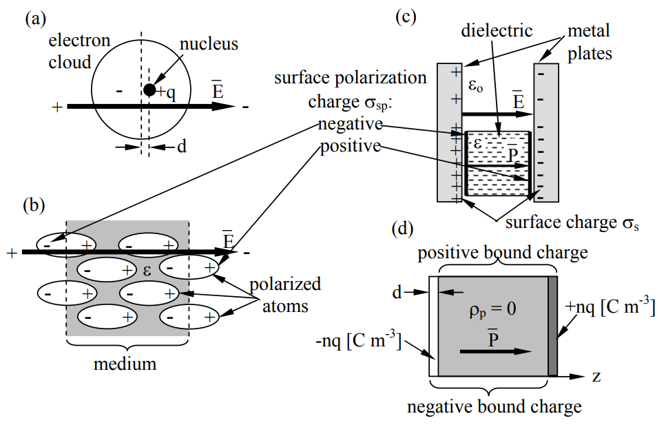
Figure 2.5.1(c) suggests how two charged plates might provide an electric field →E that polarizes a dielectric slab having permittivity ε > εo. [The electric field →E is the same in vacuum as it is inside the dielectric (assuming no air gaps) because the path integral of →E∙d→s from plate to plate equals their voltage difference V in both cases. The electric displacement overlinetor →De=ε→E and therefore differs.] We associate the difference between →Do=εo→E (vacuum) and →Dε=ε→E (dielectric) with the electric polarization overlinetor →P, where:
→D=ε→E=εo→E+→P=εo→E(1+χ)
The polarization overlinetor →P is defined by (2.5.8) and is normally parallel to →E in the same direction, as shown in Figure 2.5.1(c); it points from the negative surface polarization charge to the positive surface polarization charge (unlike →E, which points from positive charges to negative ones). As suggested in (2.5.8), →P=→EεOχ, where χ is defined as the dimensionless susceptibility of the dielectric. Because nuclei are bound rather tightly to their electron clouds, χ is generally less than 3 for most atoms, although some molecules and crystals, particularly in fluid form, can exhibit much higher values. It is shown later in (2.5.13) that →P simply equals the product of the number density n of these dipoles and the average overlinetor electric dipole moment of each atom or molecule, →p=q→d, where →d is the offset (meters) of the positive charge relative to the negative charge:
→P= nqd →d[Cm−2]
where ρf is the free charge density [C m-3]
We can derive a relation similar to (2.5.10) for →P by treating materials as distributed bound positive and negative charges with vacuum between them; the net bound charge density is designated the polarization charge density ρp [C m-3]. Then in the vacuum between the charges →D=εo→E and (2.5.10) becomes:
εo∇∙→E=ρf+ρp
From ∇ • (2.5.8), we obtain ∇∙→D=εO∇∙→E+∇∙→P=ρf. Combining this with (2.5.11) yields:
∇∙→P=−ρp
The negative sign in (2.5.12) is consistent with the fact that →P, unlike →E, is directed from negative to positive polarization charge, as noted earlier.
Outside a polarized dielectric the polarization →P is zero, as suggested by Figure 2.5.1(d). Note that the net polarization charge density is ±nq for only an atomic-scale distance d at the boundaries of the dielectric, where we model the positive and negative charge distributions within the medium as continuous uniform rectilinear slabs of density ± nq [C m-3]. These two slabs are offset by the distance d. If →P is in the z direction and arises from n dipole moments →p=q→d per cubic meter, where →d is the offset [m] of the positive charge relative to the negative charge, then (2.5.12) can be integrated over a volume V that encloses a unit area of the left-hand face of a polarized dielectric [see Figure 2.5.1(d)] to yield the polarization overlinetor →P inside the dielectric:
→P=∫V∇∙→Pdv=−∫Vρpdv=nq→d
The first equality of (2.5.13) involving →P follows from Gauss’s divergence theorem: ∫V∇∙ˉPdv=∫AˉP∙ˆzda=Pzz if A = 1. Therefore, →P=nq→d, proving (2.5.9).
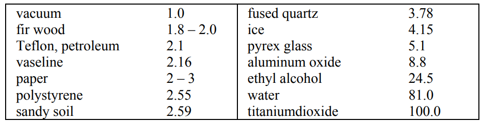
When the electric displacement →D overlineies with time it becomes displacement current, ∂→D/∂t [A/m2 ], analogous to →J, as suggested by Ampere's law: ∇×ˉH=ˉJ+∂ˉD/∂t. For reference, Table 2.5.2 presents the dielectric constants ε/εo for some common materials near 1 MHz, after Von Hippel (1954).
Table 2.5.2: Dielectric constants ε/εo of common materials near 1 MHz.
Most dielectric materials are lossy because oscillatory electric fields dither the directions and magnitudes of the induced electric dipoles, and some of this motion heats the dielectric. This effect can be represented by a frequency-dependent complex permittivity ε_, as discussed further in Section 9.5. Some dielectrics have direction-dependent permittivities that can be represented by ˉˉε; such anisotropic materials are discussed in Section 9.6. Lossy anisotropic materials can be characterized by ˉˉε_.
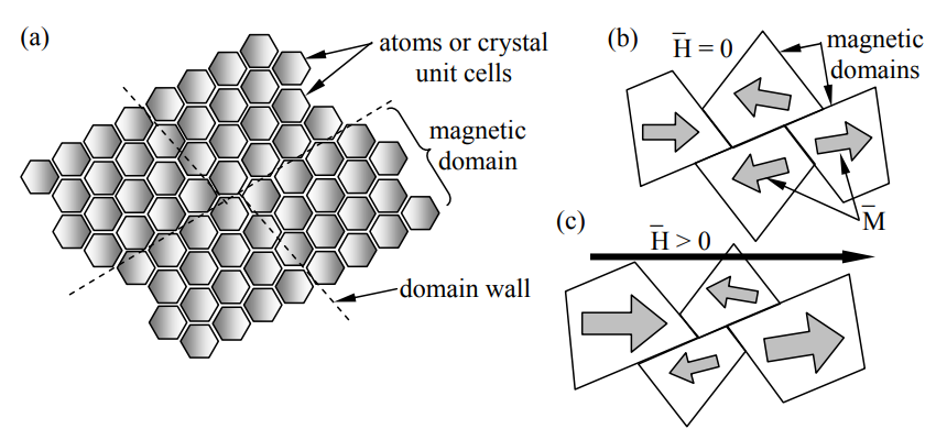
Some special dielectric media are spontaneously polarized, even in the absence of an externally applied →E. This occurs for highly polarizable media where orientation of one electric dipole in the media can motivate its neighbors to orient themselves similarly, forming domains of atoms, molecules, or crystal unit cells that are all polarized the same. Such spontaneously polarized domains are illustrated for magnetic materials in Figure 2.5.2. As in the case of ferromagnetic domains, in the absence of externally applied fields, domain size is limited by the buildup of stored field energy external to the domain; adjacent domains are oriented so as to largely cancel each other. Such ferroelectric materials have large effective values of ε, although →D saturates if →E is sufficient to produce ~100% alignment of polarization. They can also exhibit hysteresis as do the ferromagnetic materials discussed in Section 2.5.4.
What are the free and polarization charge densities ρf and ρp in a medium having conductivity σ=σo(1+z) , permittivity ε = 3εo , and current density →J=ˆzJo?
Solution
→J=σ→E, so →E=ˆzJo(1+z)/σo=εo→E+→P.
From (2.5.10) ρf=∇∙→D=(∂/∂z)[3εoJo(1+z)/σo]=3εoJo/σo [Cm−3]
From (2.5.12) ρp=−∇∙→P=−∇∙(ε−εo)→E=−(∂/∂z)2εoJo(1+z)/σo
=2εoJo/σo [Cm−3]
Permeability
The permeability μo of free space is 4π10-7 o Henries/meter by definition, where →B=μ→H. The permeability μ of matter includes the additional contributions to B from atomic magnetic dipoles aligning with the applied →H. These magnetic dipoles and their associated magnetic fields arise either from electrons orbiting about atomic nuclei or from spinning charged particles, where such moving charge is current. All electrons and protons have spin ±1/2 in addition to any orbital spin about the nucleus, and the net spin of an atom or nucleus can be non-zero. Their magnetic fields are linked to their equivalent currents by Ampere’s law, ∇×→H=→J+∂→D/∂t. Quantum theory describes how these magnetic moments are quantized at discrete levels, and for some devices quantum descriptions are necessary. In this text we average over large numbers of atoms, so that →B=μ→H accurately characterizes media, and quantum effects can be ignored.
In any medium the cumulative contribution of induced magnetic dipoles to →B is characterized by the magnetization →M, which is defined by:
→B=μ→H=μo(→H+→M)=μo→H(1+χm)
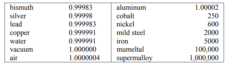
where χm is the magnetic susceptibility of the medium. Because of quantum effects χm for diamagnetic materials is slightly negative so that μ < μo; examples include silver, copper, and water, as listed in Table 2.5.3. The table also lists representative paramagnetic materials, which have slightly positive magnetic susceptibilities, and ferromagnetic materials, which have very large susceptibilities (e.g., cobalt, etc.).
Table 2.5.3: Approximate relative permeabilities μ/μo of common materials.
At sufficiently high magnetic fields all domains will expand to their maximum size and/or rotate in the direction of →H. This corresponds to the maximum value of →M and magnetic saturation. The resulting typical non-linear behavior of the magnetization curve relating B and H for ferromagnetic materials is suggested in Figure 2.5.3(a). The slope of the B vs. H curve is ~μ near the origin and ~μo beyond saturation. If the domains resist change and dissipate energy when doing so, the hysteresis curve of Figure 2.5.3(b) results. It can be shown that the area enclosed by the figure is the energy dissipated per cycle as the applied →H oscillates.
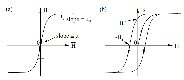
Hard magnetic materials have large values of residual flux density Br and magnetic coercive force or coercivity Hc, as illustrated. Br corresponds to the magnetic strength B of this permanent magnet with no applied H. The magnetic energy density Wm=→B∙→H/2≅0 inside permanent magnets because →H = 0 , while Wm=μoH2/2 [Jm−3] outside. To demagnetize a permanent magnet we can apply a magnetic field H of magnitude Hc, which is the field strength necessary to drive B to zero.
If we represent the magnetic dipole moment of an atom by →m, where m for a current loop of magnitude I and area ˆnA is ˆnIA [Am]7, then it can be shown that the total magnetization →M of a medium is n→m [Am−1] via the same approach used to derive →P=n→p (2.5.13) for the polarization of dielectrics; n is the number of dipoles per m3 .
Show how the power dissipated in a hysteretic magnetic material is related to the area circled in Figure 2.5.3(b) as H oscillates. For simplicity, approximate the loop in the figure by a rectangle bounded by ±Ho and ±Bo.
Solution
We seek the energy dissipated in the material by one traverse of this loop as H goes from +Ho to -Ho and back to +Ho. The energy density Wm = BH/2 when B = 0 at t =0 is Wm = 0; Wm →BoHo /2 [J m-3] as B→Bo. As H returns to 0 while B = Bo, this energy is dissipated and cannot be recovered by an external circuit because any voltage induced in that circuit would be ∝ ∂B/∂t = 0. As H→-Ho, Wm→BoHo/2; this energy can be recovered by an external circuit later as B→0 because ∂B/∂t ≠ 0. As B→-Bo, Wm→BoHo/2, which is lost later as H→0 with ∂B/∂t = 0. The energy stored as H→Ho with B = -Bo is again recoverable as B→0 with H = Ho. Thus the minimum energy dissipated during one loop traverse is vBoHo [J], where v is material volume. If the drive circuits do not recapture the available energy but dissipate it, the total energy dissipated per cycle is doubled.