
3.1: Resistors and Capacitors


- Last updated
- Jun 7, 2025
- Save as PDF

( \newcommand{\kernel}{\mathrm{null}\,}\)
Introduction
One important application of electromagnetic field analysis is to simple electronic components such as resistors, capacitors, and inductors, all of which exhibit at higher frequencies characteristics of the others. Such structures can be analyzed in terms of their: 1) static behavior, for which we can set ∂/∂t = 0 in Maxwell’s equations, 2) quasistatic behavior, for which ∂/∂t is non-negligible, but we neglect terms of the order ∂2 /∂t2 , and 3) dynamic behavior, for which terms on the order of ∂2 /∂t2 are not negligible either; in the dynamic case the wavelengths of interest are no longer large compared to the device dimensions. Because most such devices have either cylindrical or planar geometries, as discussed in Sections 1.3 and 1.4, their fields and behavior are generally easily understood. This understanding can be extrapolated to more complex structures.
One approach to analyzing simple structures is to review the basic constraints imposed by symmetry, Maxwell’s equations, and boundary conditions, and then to hypothesize the electric and magnetic fields that would result. These hypotheses can then be tested for consistency with any remaining constraints not already invoked. To illustrate this approach resistors, capacitors, and inductors with simple shapes are analyzed in Sections 3.1–2 below.
All physical elements exhibit varying degrees of resistance, inductance, and capacitance, depending on frequency. This is because: 1) essentially all conducting materials exhibit some resistance, 2) all currents generate magnetic fields and therefore contribute inductance, and 3) all voltage differences generate electric fields and therefore contribute capacitance. R’s, L’s, and C’s are designed to exhibit only one dominant property at low frequencies. Section 3.3 discusses simple examples of ambivalent device behavior as frequency changes.
Most passive electronic components have two or more terminals where voltages can be measured. The voltage difference between any two terminals of a passive device generally depends on the histories of the currents through all the terminals. Common passive linear twoterminal devices include resistors, inductors, and capacitors (R’s, L’s. and C’s, respectively), while transformers are commonly three- or four-terminal devices. Devices with even more terminals are often simply characterized as N-port networks. Connected sets of such passive linear devices form passive linear circuits which can be analyzed using the methods discussed in Section 3.4. RLC resonators and RL and RC relaxation circuits are most relevant here because their physics and behavior resemble those of common electromagnetic systems. RLC resonators are treated in Section 3.5, and RL, RC, and LC circuits are limiting cases when one of the three elements becomes negligible.
Resistors
Resistors are two-terminal passive linear devices characterized by their resistance R [ohms]:
v=iR
where v(t) and i(t) are the associated voltage and current. That is, one volt across a one-ohm resistor induces a one-ampere current through it; this defines the ohm.
The resistor illustrated in Figure 3.1.1 is comprised of two parallel perfectly conducting endplates between which is placed a medium of conductivity σ, permittivity ε, permeability μ, and thickness d; the two end plates and the medium all have a constant cross-sectional area A [m2 ] in the x-y plane. Let’s assume a static voltage v exists across the resistor R, and that a current i flows through it.
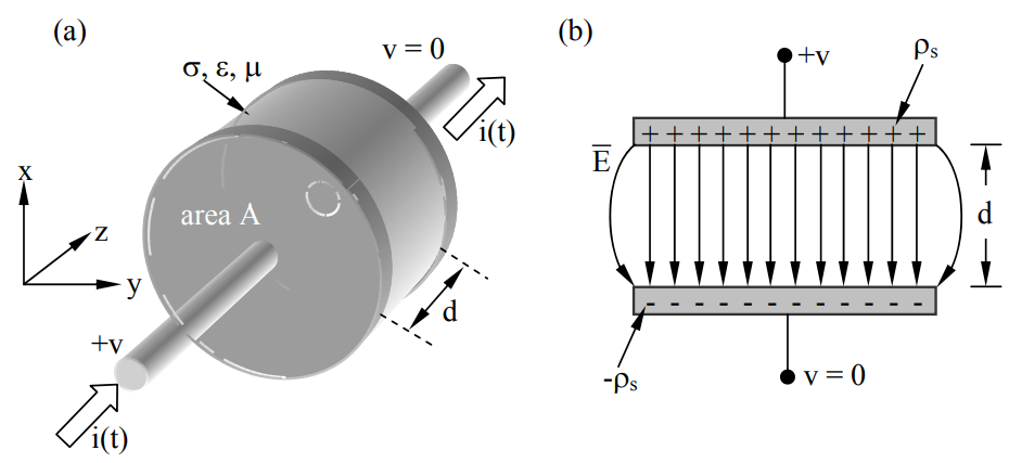
Boundary conditions require the electric field→Eat any perfectly conducting plate to be perpendicular to it [see (2.6.16); →E׈n=0] , and Faraday’s law requires that any line integral of→Efrom one iso-potential end plate to the other must equal the voltage v regardless of the path of integration (1.3.13). Because the conductivity σ [Siemens/m] is uniform within walls parallel to ˆz, these constraints are satisfied by a static uniform electric field →E=ˆzEo everywhere within the conducting medium, which would be charge-free since our assumed→Eis non-divergent. Thus:
∫d0→E∙ˆzdz=E0d=v
where Eo=v/d[Vm−1].
Such an electric field within the conducting medium induces a current density →J, where:
→J=σ→E[Am−2]
The total current i flowing is the integral of →J∙ˆz over the device cross-section A, so that:
i=∫∫A→J∙ˆzdxdy=∫∫Aσ→E∙ˆzdxdy=∫∫AσEodxdy=σEoA=vσA/d
But i = v/R from (3.1.1), and therefore the static resistance of a simple planar resistor is:
R=v/i=d/σA [ohms]
The instantaneous power p [W] dissipated in a resistor is i2R = v2/R, and the time-average power dissipated in the sinusoidal steady state is |I_|2R/2=|V_|2/2R watts. Alternatively the local instantaneous power density can be integrated over the volume of the resistor to yield the total instantaneous power dissipated:
which is the expected answer, and where we used (2.1.17): .
Surface charges reside on the end plates where the electric field is perpendicular to the perfect conductor. The boundary condition suggests that the surface charge density ρs on the positive end-plate face adjacent to the conducting medium is:
The total static charge Q on the positive resistor end plate is therefore ρsA coulombs. By convention, the subscript s distinguishes surface charge density ρs [C m-2] from volume charge density ρ [C m-3]. An equal negative surface charge resides on the other end-plate. The total stored charged Q = ρsA = CV, where C is the device capacitance, as discussed further in Section 3.1.3.
The static currents and voltages in this resistor will produce fields outside the resistor, but these produce no additional current or voltage at the device terminals and are not of immediate concern here. Similarly, μ and ε do not affect the static value of R. At higher frequencies, however, this resistance R varies and both inductance and capacitance appear, as shown in the following three sections. Although this static solution for charge, current, and electric field within the conducting portion of the resistor satisfies Maxwell’s equations, a complete solution would also prove uniqueness and consistency with →H and Maxwell’s equations outside the device. Uniqueness is addressed by the uniqueness theorem in Section 2.8, and approaches to finding fields for arbitrary device geometries are discussed briefly in Sections 4.4–6.
Design a practical 100-ohm resistor. If thermal dissipation were a problem, how might that change the design?
Solution
Resistance R = d/σA (3.1.5), and if we arbitrarily choose a classic cylindrical shape with resistor length d = 4r, where r is the radius, then A = πr2 = πd2 /16 and R = 16/πdσ = 100. Discrete resistors are smaller for modern low power compact circuits, so we might set d = 1 mm, yielding σ = 16/πdR = 16/(π10-3×100) ≅ 51 S m-1. Such conductivities roughly correspond, for example, to very salty water or carbon powder. The surface area of the resistor must be sufficient to dissipate the maximum power expected, however. Flat resistors thermally bonded to a heat sink can be smaller than air-cooled devices, and these are often made of thin metallic film. Some resistors are long wires wound in coils. Resistor failure often occurs where the local resistance is slightly higher, and the resulting heat typically increases the local resistance further, causing even more local heating.
Capacitors
Capacitors are two-terminal passive linear devices storing charge Q and characterized by their capacitance C [Farads], defined by:
Q=Cv [ Coulombs ]
where v(t) is the voltage across the capacitor. That is, one static volt across a one-Farad capacitor stores one Coulomb on each terminal, as discussed further below; this defines the Farad [Coulombs per volt].
The resistive structure illustrated in Figure 3.1.1 becomes a pure capacitor at low frequencies if the media conductivity σ → 0. Although some capacitors are air-filled with ε ≅ εo, usually dielectric filler with permittivity ε > εo is used. Typical values for the dielectric constant ε/εo used in capacitors are ~1-100. In all cases boundary conditions again require that the electric field E be perpendicular to the perfectly conducting end plates, i.e., to be in the ±z direction, and Faraday’s law requires that any line integral of E from one iso-potential end plate to the other must equal the voltage v across the capacitor. These constraints are again satisfied by a static uniform electric field →E=ˆzEo within the medium separating the plates, which is uniform and charge-free.
We shall neglect temporarily the effects of all fields produced outside the capacitor if its plate separation d is small compared to its diameter, a common configuration. Thus Eo = v/d [V m-1] (3.1.2). The surface charge density on the positive end-plate face adjacent to the conducting medium is σs = εEo [C m-2], and the total static charge Q on the positive end plate of area A is therefore:
Q=Aσs=AεEo=Aεv/d=Cv [C]
Therefore, for a parallel-plate capacitor:
C=εA/d [ Farads ](parallel-plate capacitor)
Using (3.1.2) and the fact that the charge Q(t) on the positive plate is the time integral of the current i(t) into it, we obtain the relation between voltage and current for a capacitor:
v(t)=Q(t)/C=(1/C)∫t−∞i(t)dt
i(t)=Cdv(t)/dt
When two capacitors are connected in parallel as shown in Figure 3.1.2, they are equivalent to a single capacitor of value Ceq storing charge Qeq, where these values are easily found in terms of the charges (Q1, Q2) and capacitances (C1, C2) associated with the two separate devices.
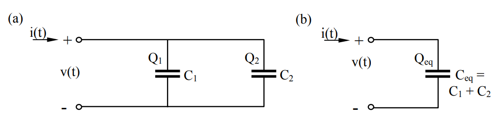
Because the total charge Qeq is the sum of the charges on the two separate capacitors, and capacitors in parallel have the same voltage v, it follows that:
Qeq=Q1+Q2=(C1+C2)v=Ceqv
Ceq=C1+C2 (capacitors in parallel)
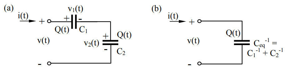
When two capacitors are connected in series, as illustrated in Figure 3.1.3, then their two charges Q1 and Q2 remain equal if they were equal before current i(t) began to flow, and the total voltage is the sum of the voltages across each capacitor:
C−1eq=v/Q=(v1+v2)/Q=C−11+C−12 (capacitors in series)
The instantaneous electric energy density We [J m-3] between the capacitor plates is given by Poynting’s theorem: We=ε|→E|2/2 (2.7.7). The total electric energy we stored in the capacitor is the integral of We over the volume Ad of the dielectric:
we=∫∫∫V(ε|→E|2/2)dv=εAd|→E|2/2=εAv2/2d=Cv2/2 [J]
The corresponding expression for the time-average energy stored in a capacitor in the sinusoidal steady state is:
we=C|J_|2/4 [V]
The extra factor of two relative to (3.1.9) enters because the time average of a sinsuoid squared is half its peak value.
To prove (3.1.16) for any capacitor C, not just parallel-plate devices, we can compute we=∫t0ivdt where i = dq/dt and q = Cv Therefore we=∫t0C(dv/dt)vdt=∫v0Cvdv=Cv2/2 in general.
We can also analyze other capacitor geometries, such as the cylindrical capacitor illustrated in Figure 3.1.4. The inner radius is “a”, the outer radius is “b”, and the length is D; its interior has permittivity ε.
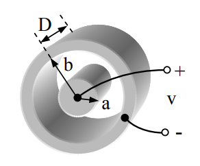
The electric field again must be divergence- and curl-free in the charge-free regions between the two cylinders, and must be perpendicular to the inner and outer cylinders at their perfectly conducting walls. The solution can be cylindrically symmetric and independent of ϕ. A purely radial electric field has these properties:
→E(r)=ˆrEo/r
The electric potential Φ(r) is the integral of the electric field, so the potential difference v between the inner and outer conductors is:
v=Φa−Φb=∫baEordr=Eolnr|ba=Eoln(ba) [V]
This capacitor voltage produces a surface charge density ρs on the inner and outer conductors, where ρs=εE=εEo/r. If Φa>Φb, then the inner cylinder is positively charged, the outer cylinder is negatively charged, and Eo is positive. The total charge Q on the inner cylinder is then:
Q=ρs2πaD=εEo2πD=εv2πD/[ln(b/a)]=CC [v]
Therefore this cylindrical capacitor has capacitance C:
C=ε2πD/[ln(b/a)][F] (cylindrical capacitor)
In the limit where b/a → 1 and b - a = d, then we have approximately a parallel-plate capacitor with C → εA/d where the plate area A = 2πaD; see (3.1.10).
Design a practical 100-volt 10-8 farad (0.01 mfd) capacitor using dielectric having ε = 20εo and a breakdown field strength EB of 107 [V m-1].
Solution
For parallel-plate capacitors C = εA/d (3.1.10), and the device breakdown voltage is EBd = 100 [V]. Therefore the plate separation d = 100/EB = 10-5 [m]. With a safety factor of two, d doubles to 2×10⁻⁵, so A = dC/ε = 2×10-5 × 10-8/(20 × 6.85×10-12) ≅ 1.5×10³ [m2]. If the capacitor is a cube of side D, then the capacitor volume is D3 = Ad and D = (Ad)0.333 = (1.5×10-3 × 2×10-5)0.333 ≅ 3.1 mm. To simplify manufacture, such capacitors are usually wound in cylinders or cut from flat stacked sheets.