
6.4: Charge Carriers in Semiconductors - Statics and Kinetics


- Last updated
- Sep 20, 2022
- Save as PDF

( \newcommand{\kernel}{\mathrm{null}\,}\)
Now let me demonstrate the application of the concepts discussed in the last section to understanding the basic kinetic properties of semiconductors and a few key semiconductor structures – which are the basis of most modern electronic and optoelectronic devices, and hence of all our IT civilization. For that, I will need to take a detour to discuss their equilibrium properties first.
I will use an approximate but reasonable picture in which the energy of the electron subsystem in a solid may be partitioned into the sum of effective energies ε of independent electrons. Quantum mechanics says32 that in such periodic structures as crystals, the stationary state energy ε of a particle interacting with the atomic lattice follows one of periodic functions εn(q) of the quasimomentum q, oscillating between two extreme values εn|min and εn|max. These allowed energy bands are separated by bandgaps, of widths Δn≡εn|min–εn−1|max, with no allowed states inside them. Semiconductors and insulators (dielectrics) are defined as such crystals that in equilibrium at T=0, all electron states in several energy bands (with the highest of them called the valence band) are completely filled, ⟨N(εv)⟩=1, while those in the upper bands, starting from the lowest, conduction band, are completely empty, ⟨N(εc)⟩=0.33 Since the electrons follow the Fermi-Dirac statistics (2.8.5), this means that at T→0, the Fermi energy εF≡μ(0) is located somewhere between the valence band's maximum εv|max (usually called simply εV), and the conduction band's minimum εc|min (called εC) – see Figure 6.4.1.
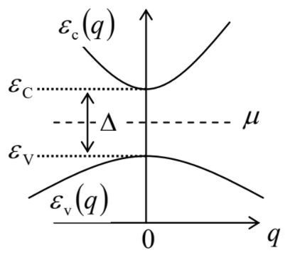
ε={εc+q2/2mc, for ε≥εc, with εc−εv≡Δ.εv+q2/2mv, for ε≥εc, with εc−εv≡Δ.
The positive constants mC and mV are usually called the effective masses of, respectively, electrons and holes. (In a typical semiconductor, mC is a few times smaller than the free electron mass me, while mV is closer to me.)
Due to the similarity between the top line of Equation (???) and the dispersion law (3.1.3) of free particles, we may re-use Equation (3.2.11), with the appropriate particle mass m, the degeneracy factor g, and the energy origin, to calculate the full spatial density of populated states (in semiconductor physics, called electrons in the narrow sense of the word):
n≡NcV=∫∞εC⟨N(ε)⟩g3(ε)dε≡gcm3/2c√2π2ℏ3∫∞0⟨N(˜ε+εC)⟩∼E1/2d˜ε,
where ˜ε≡ε–εC≥0. Similarly, the density p of “no-electron” excitations (called holes) in the valence band is the number of unfilled states in the band, and hence may be calculated as
p≡NhV=∫εv−∞[1−⟨N(ε)⟩]g3(ε)dε≡gvm3/2v√2π2ℏ3∫∞0[1−⟨N(εv−˜ε)⟩]˜ε1/2d˜ε,
where in this case, ˜ε≥0 is defined as (εV–ε). If the electrons and holes35 are in the thermal and chemical equilibrium, the functions ⟨N(ε)⟩ in these two relations should follow the Fermi-Dirac distribution (2.8.5) with the same temperature T and the same chemical potential μ. Moreover, in our current case of an undoped (intrinsic) semiconductor, these densities have to be equal,
n=p≡ni,
because if this electroneutrality condition was violated, the volume would acquire a non-zero electric charge density ρ=e(p–n), which would result, in a bulk sample, in an extremely high electric field energy. From this condition, we get a system of two equations,
ni=gCm3/2c√2π2ℏ3∫∞0˜ε1/2d˜εexp{(˜ε+εc−μ)/T}+1=gVm3/2V√2π2ℏ3∫∞0˜ε1/2d˜εexp{(˜ε−εV+μ)/T}+1
whose solution gives both the requested charge carrier density ni and the Fermi level μ.
For an arbitrary ratio Δ/T, this solution may be found only numerically, but in most practical cases, this ratio is very large. (Again, for Si at room temperature, Δ≈1.14 eV, while T≈0.025 eV.) In this case, we may use the same classical approximation as in Equation (3.2.16), to reduce Eqs. (???) and (???) to simple expressions
n=ncexp{μ−εcT},p=nvexp{εv−μT}, for T<<Δ,
where the temperature-dependent parameters
nc≡gcℏ3(mcT2π)3/2 and nv≡gvℏ3(mvT2π)3/2
may be interpreted as the effective numbers of states (per unit volume) available for occupation in, respectively, the conduction and valence bands, in thermal equilibrium. For usual semiconductors (with gC∼gV∼1, and mC∼mV∼me), at room temperature, these numbers are of the order of 3×1025m−3≡3×1019cm−3. (Note that all results based on Eqs. (???) are only valid if both n and p are much lower than, respectively, nC and nV.)
With the substitution of Eqs. (???), the system of equations (???) allows a straightforward solution:
μ=εv+εc2+T2(lngvgc+3lnmvmc),ni=(ncnv)1/2exp{−Δ2T}.
Since in all practical materials the logarithms in the first of these expressions are never much larger than 1,36 it shows that the Fermi level in intrinsic semiconductors never deviates substantially from the so called midgap value (εV+εC)/2 – see the (schematic) Figure 6.4.1. In the result for ni, the last (exponential) factor is very small, so that the equilibrium number of charge carriers is much lower than that of the atoms – for the most important case of silicon at room temperature, ni∼1010cm−3. The exponential temperature dependence of ni (and hence of the electric conductivity σ∝ni) of intrinsic semiconductors is the basis of several applications, for example simple germanium resistance thermometers, efficient in the whole range from ∼0.5 K to ∼100 K. Another useful application of the same fact is the extraction of the bandgap of a semiconductor from the experimental measurement of the temperature dependence of σ∝ni – frequently, in just two well-separated temperature points.
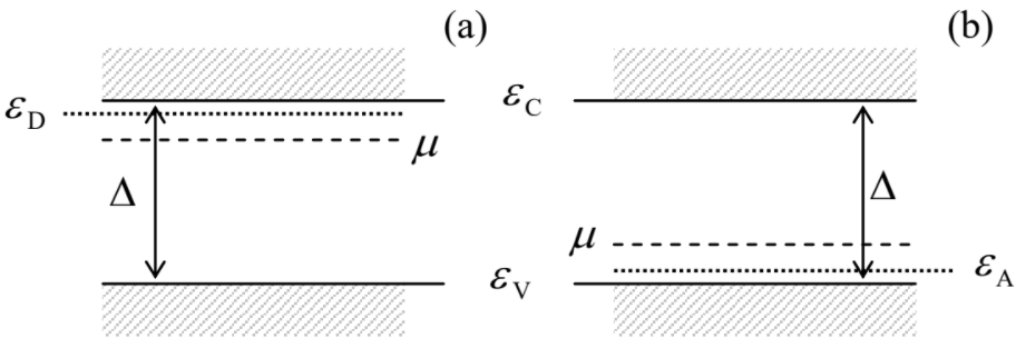
However, most applications require a much higher concentration of carriers. It may be increased quite dramatically by planting into a semiconductor a relatively small number of slightly different atoms – either donors (e.g., phosphorus atoms for Si) or acceptors (e.g., boron atoms for Si). Let us analyze the first opportunity, called n-doping, using the same simple energy band model (???). If the donor atom is only slightly different from those in the crystal lattice, it may be easily ionized – giving an additional electron to the conduction band, and hence becoming a positive ion. This means that the effective ground state energy εD of the additional electrons is just slightly below the conduction band edge εC – see Figure 6.4.2a.37
np=n2i.
However, for a doped semiconductor, the electroneutrality condition looks differently from Equation (???), because the total density of positive charges in a unit volume is not p, but rather (p+n+), where n+ is the density of positively-ionized (“activated”) donor atoms, so that the electroneutrality condition becomes
n=p+n+.
If virtually all dopants are activated, as it is in most practical cases,39 then we may take n+=nD, where nD is the total concentration of donor atoms, i.e. their number per unit volume, and Equation (???) becomes
n=p+nD.
Plugging in the expression p=n2i/n, following from Equation (???), we get a simple quadratic equation for n, with the following physically acceptable (positive) solution:
n=nD2+(n2D4+n2i)1/2.
This result shows that the doping affects n (and hence μ=εC–Tln(nC/n) and p=n2i/n) only if the dopant concentration nD is comparable with, or higher than the intrinsic carrier density ni given by Equation (???). For most applications, nD is made much higher than ni; in this case Equation (???) yields
n≈nD>>ni,p=n2in≈n2inD<<n,μ≈μp≡εC−TlnnCnD.
Because of the reasons to be discussed very soon, modern electron devices require doping densities above 1018cm−3, so that the logarithm in Equation (???) is not much larger than 1. This means that the Fermi level rises from the midgap to a position only slightly below the conduction band edge εC – see Figure 6.4.2a.
The opposite case of purely p-doping, with nA acceptor atoms per unit volume, and a small activation (negative ionization) energy εA–εV<<Δ,40 may be considered absolutely similarly, using the electroneutrality condition in the form
n+n=p−,
where n– is the number of activated (and hence negatively charged) acceptors. For the relatively high concentration (ni<<nA<<nV), virtually all acceptors are activated, so that n–≈nA, Equation (???) may be approximated as n+nA=p, and the analysis gives the results dual to Equation (???):
p≈nA>>ni,n=n2ip≈n2inA<<p,μ≈μn≡εV+TlnnVnA.
so that in this case, the Fermi level is just slightly above the valence band edge (Figure 6.4.2b), and the number of holes far exceeds that of electrons – again, in the narrow sense of the word. Let me leave the analysis of the simultaneous n- and p-doping (which enables, in particular, so-called compensated semiconductors with the sign-variable difference n–p≈nD–nA) for the reader's exercise.
d2ϕdx2=−ρ(x)κε0.
Here κ is the dielectric constant of the semiconductor matrix – excluding the dopants and charge carriers, which in this approach are treated as explicit (“stand-alone”) charges, with the volumic density
ρ=e(pn−−n).
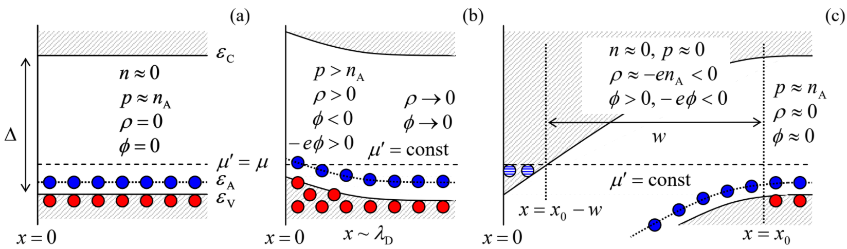
(As a sanity check, Eqs. (???)-(???) show that if E≡–dϕ/dx=0, then ρ=0, bringing us back to the electroneutrality condition (???), and hence the “flat” band-edge diagrams shown in Figs. 6.4.2b and 6.4.3a.)
dϕdx(0)=−E.
Note that the electrochemical potential μ′ (which, in accordance with the discussion in Sec. 3, replaces the chemical potential in presence of the electric field),46 has to stay constant through the system in equilibrium, keeping the electric current equal to zero – see Equation (6.3.6). For arbitrary doping parameters, the system of equations (???) (with the replacements εV→εV–eϕ, and μ→μ′) and (???)-(???), plus the relation between n– and nA (describing the acceptor activation), does not allow an analytical solution. However, as was discussed above, in the most practical cases nA>>ni, we may use the approximate relations n–≈nA and n≈0 at virtually any values of μ′ within the locally shifted bandgap [εV–eϕ(x),εC–eϕ(x)], so that the substitution of these relations, and the second of Eqs. (???), with the mentioned replacements, into Equation (???) yields
ρ≈enVexp{εV−eϕ−μ′T}−enA≡enA[(nVnVexp{εV−μ′T})exp{−eϕT}−1].
The x-independent electrochemical potential (a.k.a. Fermi level) μ′ in this relation should be equal to the value of the chemical potential μ(x→∞) in the semiconductor's bulk, given by the last of Eqs. (???), which turns the expression in the parentheses into 1. With these substitutions, Equation (???) becomes
d2ϕdx2=−enAκε0[exp{−eϕT}−1], for εV−eϕ(x)<μ′<εC−eϕ(x).
This nonlinear differential equation may be solved analytically, but in order to avoid a distraction by this (rather bulky) solution, let me first consider the case when the electrostatic potential is sufficiently small – either because the external field is small, or because we focus on the distances sufficiently far from the surface – see Figure 6.4.3 again. In this case, in the Taylor expansion of the exponent in Equation (???), with respect to small ϕ, we may keep only two leading terms, turning it into a linear equation:
d2ϕdx2=−e2nAκε0Tϕ, i.e. d2ϕdx2=ϕλ2D, where λD≡(κε0Te2nA)1/2,
with the well-known exponential solution, satisfying also the boundary condition ϕ→0 at x→∞:
ϕ=Cexp{−xλD}, at e|ϕ|<<T.
The constant λD given by the last of Eqs. (???) is called the Debye screening length. It may be rather substantial; for example, at TK=300 K, even for the relatively high doping, nA≈1018cm−3 typical for modern silicon (κ≈12) integrated circuits, it is close to 4 nm – still much larger than the crystal lattice constant a∼0.3 nm, so that the above analysis is indeed quantitatively valid. Note also that λD does not depend on the charge's sign; hence it should be no large surprise that repeating our analysis for an n-doped semiconductor, we may find out that Eqs. (???)-(???) are valid for that case as well, with the only replacement nA→nD.
If the applied field E is weak, Equation (???) is valid in the whole sample, and the constant C in it may be readily calculated using the boundary condition (???), giving
|ϕ|x=0≡C=λDE≡(κε0Te2nA)1/2E.
This formula allows us to express the condition of validity of the linear approximation leading to Equation (???), e|ϕ|<<T, in terms of the applied field:
|E|<<Emax, with Emax≡TeλD≡(TnAκε0)1/2;
in the above example, Emax∼60 kV/cm. On the lab scale, such field is not low at all (it is twice higher than the threshold of electric breakdown in the air at ambient conditions), but may be sustained by many solid-state materials that are much less prone to the breakdown.47 This is why we should be interested in what happens if the applied field is higher than this value.
λef(0)∼λTF≡[κε0e2g3(εF)]1/2.
The effects taking place at the opposite polarity of the field, E>0, are much more interesting – and more useful for applications. Indeed, in this case, the band bending down leads to an exponential decrease of ρ(x) as soon as the valence band edge εV–eϕ(x) drops down by just a few T below its unperturbed value εV. If the applied field is large enough, E>Emax (as it is in the situation shown in Figure 6.4.3c), it forms, on the left of such point x0 the so-called depletion layer, of a certain width w. Within this layer, not only the electron density n, but the hole density p as well, are negligible, so that the only substantial contribution to the charge density ρ is given by the fully ionized acceptors: ρ≈–en–≈–enA, and Equation (???) becomes very simple:
d2ϕdx2=enAκε0=const, for x0−w<x<x0.
Let us use this equation to calculate the largest possible width w of the depletion layer, and the critical value, Ec, of the applied field necessary for this. (By definition, at E=Ec, the left boundary of the layer, where εV–eϕ(x)=εC, i.e. eϕ(x)=εV–εA≡Δ, just touches the semiconductor surface: x0–w=0, i.e. x0=w. (Figure 6.4.3c shows the case when E is slightly larger than Ec.) For this, Equation (???) has to be solved with the following boundary conditions:
ϕ(0)=Δe,dϕdx(0)=−Ec,ϕ(w)=0,dϕdx(w)=0.
Note that the first of these conditions is strictly valid only if T<<Δ, i.e. at the assumption we have made from the very beginning, while the last two conditions are asymptotically correct only if λD<<w – the assumption we should not forget to check after the solution.
After all the undergraduate experience with projective motion problems, the reader certainly knows by heart that the solution of Equation (???) is a quadratic parabola, so that let me immediately write its final form satisfying the boundary conditions (???):
ϕ(x)=enAκε0(w−x)22, with w=(2κε0Δe2nA)1/2, at Ec=2Δeε0w.
Comparing the result for w with Equation (???), we see that if our basic condition T<<Δ is fulfilled, then λD<<w, confirming the qualitative validity of the whole solution (???). For the same particular parameters as in the example before (nA≈1018cm−3,κ≈10), and Δ≈1 eV, Eqs. (???) give w≈40 nm and Ec≈600 kV/cm – still a practicable field. (As Figure 6.4.3c shows, to create it, we need a gate voltage only slightly larger than Δ/e, i.e. close to 1 V for typical semiconductors.)
Figure 6.4.3c also shows that if the applied field exceeds this critical value, near the surface of the semiconductor the conduction band edge drops below the Fermi level. This is the so-called inversion layer, in which electrons with energies below μ′ form a highly conductive degenerate Fermi gas. However, typical rates of electron tunneling from the bulk through the depletion layer are very low, so that after the inversion layer has been created (say, by the gate voltage application), it may be only populated from another source – hence the hatched blue points in Figure 6.4.3c. This is exactly the fact used in the workhorse device of semiconductor integrated circuits – the field-effect transistor (FET) – see Figure 6.4.4.
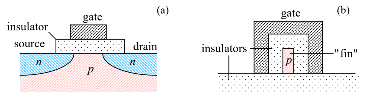
In the “bulk” variety of this structure (Figure 6.4.4a), a gate electrode overlaps a gap between two similar highly-n-doped regions near the surface, called source and drain, formed by n-doping inside a p doped semiconductor. It is more or less obvious (and will be shown in a moment) that in the absence of gate voltage, the electrons cannot pass through the p-doped region, so that virtually no current flows between the source and the drain, even if a modest voltage is applied between these electrodes. However, if the gate voltage is positive and large enough to induce the electric field E>Ec at the surface of the p-doped semiconductor, it creates the inversion layer as shown in Figure 6.4.3c, and the electron current between the source and drain electrodes may readily flow through this surface channel. (Very unfortunately, in this course I would not have time/space for a detailed analysis of transport properties of this keystone electron device, and have to refer the reader to special literature.49)
Figure 6.4.4a makes it obvious that another major (and virtually unavoidable) structure of semiconductor integrated circuits is the famous p−n junction – an interface between p- and n-doped regions. Let us analyze its simple model, in which the interface is in the plane x=0, and the doping profiles nD(x) and nA(x) are step-like, making an abrupt jump at the interface:
nA(x)={nA=const at x<0,0, at x>0,nD(x)={0 at x<0,nD=const at x>0.
(This model is very reasonable for modern integrated circuits, where the doping in performed by implantation, using high-energy ion beams.)
To start with, let us assume that no voltage is applied between the p- and n-regions, so that the system may be in thermodynamic equilibrium. In the equilibrium, the Fermi level μ′ should be flat through the structure, and at x→–∞ and x→+∞, where ϕ→0, the level structure has to approach the positions shown, respectively, on panels (a) and (b) of Figure 6.4.2. In addition, the distribution of the electric potential ϕ(x), shifting the level structure vertically by –eϕ(x), has to be continuous to avoid unphysical infinite electric fields. With that, we inevitably arrive at the band-edge diagram that is (schematically) shown in Figure 6.4.5.
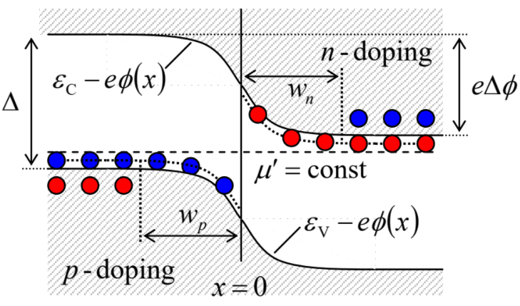
The diagram shows that the contact of differently doped semiconductors gives rise to a built-in electric potential difference Δϕ, equal to the difference of their values of μ in the absence of the contact – see Eqs. (???) and (???):
eΔϕ≡eϕ(+∞)−eϕ(−∞)=μn−μp=Δ−TlnnCnVnDnA,
which is usually just slightly smaller than the bandgap.50 (Qualitatively, this is the same contact potential difference that was discussed, for the case of metals, in Sec. 3 – see Figure 6.3.1.) The arising internal electrostatic field E=–dϕ/dx induces, in both semiconductors, depletion layers similar to that induced by an external field (Figure 6.4.3c). Their widths wp and wn may also be calculated similarly, by solving the following boundary problem of electrostatics, mostly similar to that given by Eqs. (???)-(???):
d2ϕdx2=eκε0×{nA, for −wp<x<0,(−nD), for 0<x<+wn,
ϕ(wn)=ϕ(−wp)+Δϕ,dϕdx(wn)=dϕdx(−wp)=0,ϕ(−0)=ϕ(+0),dϕdx(−0)=dϕdx(+0),
also exact only in the limit τ<<Δ,ni<<nD,nA. Its (easy) solution gives the result similar to Equation (???):
ϕ=const+{enA(wp+x)2/2κε0, for −qp<x<0,Δϕ−enD(wn−x)2/2κε0, for 0<x<+wn,
with expressions for wp and wn giving the following formula for the full depletion layer width:
w≡wp+wn=(2κε0Δϕenef)1/2, with nef≡nAnDnA+nD, i.e.1nef=1nA+1nD.
This expression is similar to that given by Equation (???), so that for typical highly doped semiconductors (nef∼1018cm−3) it gives for w a similar estimate of a few tens nm.51 Returning to Figure 6.4.4a, we see that this scale imposes an essential limit on the reduction of bulk FETs (whose scaling down is at the heart of the well-known Moore's law),52 explaining why such high doping is necessary. In the early 2010s, the problems with implementing even higher doping, plus issues with dissipated power management, have motivated the transition of advanced silicon integrated circuit technology from the bulk FETs to the FinFET (also called “double-gate”, or “tri-gate”, or “wrap-around-gate”) variety of these devices, schematically shown in Figure 6.4.4b, despite their essentially 3D structure and hence a more complex fabrication technology. In the FinFETs, the role of p−n junctions is reduced, but these structures remain an important feature of semiconductor integrated circuits.
Now let us have a look at the p−n junction in equilibrium from the point of view of Equation (6.3.19). In the simple model we are considering now (in particular, at T<<Δ), this equation is applicable separately to the electron and hole subsystems, because in this model the gases of these charge carriers are classical in all parts of the system, and the generation-recombination processes53 coupling these subsystems have relatively small rates – see below. Hence, for the electron subsystem, we may rewrite Equation (6.3.19) as
jn=nμmqE−Dn∂n∂x,
where q=–e. Let us discuss how each term of the right-hand of this equality depends on the system's parameters. Because of the n-doping at x>0, there are many more electrons in this part of the system. According to the Boltzmann distribution (???), some number of them,
n>∝exp{−eΔϕT},
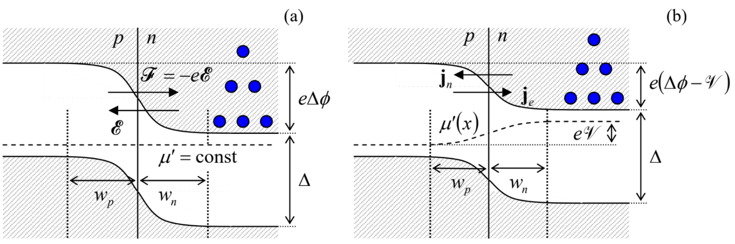
eΔϕ→eΔϕ+Δμ′≡eΔϕ+qV≡e(Δϕ−V).
This change results in an exponential change of the number of electrons able to diffuse into the p-side of the junction – cf. Equation (???):
n>(V)≈n>(0)exp{eVT},
and hence in a proportional change of the diffusion flow jn of electrons from the n-side to the p-side of the system, i.e. of the oppositely directed density of the electron current je=–ejn – see Figure 6.4.6b.
On the other hand, the drift counter-flow of electrons is not altered too much by the applied voltage: though it does change the electrostatic field E=–∇ϕ inside the depletion layer, and also the depletion layer width,57 these changes are incremental, not exponential. As the result, the net density of the current carried by electrons may be approximately expressed as
je(V)=jdiffusion−jdrift≈je(0)exp{eVT}−const.
As was discussed above, at V=0, the net current has to vanish, so that the constant in Equation (???) has to equal je(0), and we may rewrite this equality as
je(V)=je(0)(exp{eVT}−1).
j(V)≡je(V)+jh(V)=j(0)(exp{eVT}−1), with j(0)≡je(0)+jh(0),
describing the main p−n junction's property as an electric diode – a two-terminal device passing the current more “readily” in one direction (from the p- to the n-terminal) than in the opposite one.59 Besides numerous practical applications in electrical and electronic engineering, such diodes have very interesting statistical properties, in particular performing very non-trivial transformations of the spectra of deterministic and random signals. Very unfortunately, I would not have time for their discussion and have to refer the interested reader to the special literature.60
Still, before proceeding to our next (and last!) topic, let me give for the reader reference, without proof, the expression for the scaling factor j(0) in Equation (???), which follows from a simple, but broadly used model of the recombination process:
j(0)=en2i(DelenA+DhlhnD).
Here le and lh are the characteristic lengths of diffusion of electrons and holes before their recombination, which may be expressed by Equation (5.6.8), le=(2Deτe)1/2 and lh=(2Dhτh)1/2, with τe and τh being the characteristic times of recombination of the so-called minority carriers – of electrons in the p-doped part, and of holes in the n-doped part of the structure. Since the recombination is an inelastic process, its times are typically rather long – of the order of 10−7 s, i.e. much longer than the typical times of elastic scattering of the same carriers, that define their diffusion coefficients – see Equation (6.3.16-6.3.18).