
2.4: Polarization and Screening


- Last updated
- Mar 5, 2022
- Save as PDF

( \newcommand{\kernel}{\mathrm{null}\,}\)
The basic principles of electrostatics outlined in Chapter 1 present the conceptually full solution to the problem of finding the electrostatic field (and hence Coulomb forces) induced by electric charges distributed over space with density ρ(r). However, in most practical situations, this function is not known but should be found self consistently with the field. For example, if a volume of relatively dense material is placed into an external electric field, it is typically polarized, i.e. acquires some local charges of its own, which contribute to the total electric field E(r) inside, and even outside it – see Fig. 1a.
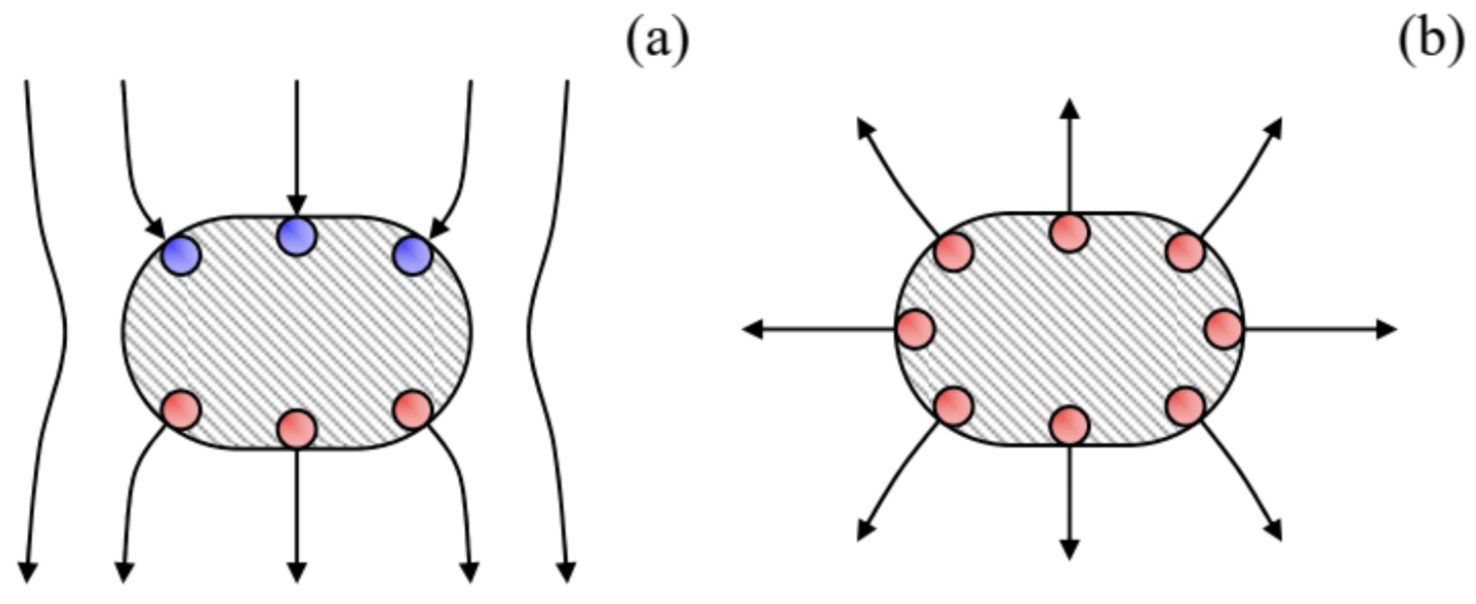 Fig. 2.1. Two typical electrostatic situations involving conductors: (a) polarization by an external field, and (b) re-distribution of conductor’s own charge over its surface –schematically. Here and below, the red and blue points denote charges of opposite signs.
The full solution of such problems should satisfy not only the fundamental Eq. (1.7) but also the so-called constitutive relations between the macroscopic variables describing the body’s material. Due to the atomic character of real materials, such relations may be very involved. In this part of my series, I will have time to address these relations, for various materials, only rather superficially,1 focusing on their simple approximations. Fortunately, in most practical cases such approximations work very well.
In particular, for the polarization of good conductors, a very reasonable approximation is given by the so-called macroscopic model, in which the free charges in the conductor are is treated as a charged continuum that is free to move under the effect of the force F=qE exerted by the macroscopic electric field E, i.e. the field averaged over the atomic scale – see also the discussion at the end of Sec. 1.1. In electrostatics (which excludes the case dc currents, to be discussed in Chapter 4 below), there should be no such motion, so that everywhere inside the conductor the macroscopic electric field should vanish:
E=0.
Conductor: macroscopic model
This is the electric field screening2 effect, meaning, in particular, that the conductor’s polarization in an external electric field has the extreme form shown (rather schematically) in Fig. 1a, with the field of the induced surface charges completely compensating the external field in the conductor’s bulk. Note that Eq. (1a) may be rewritten in another, frequently more convenient form:
ϕ=const,
where ϕ is the macroscopic electrostatic potential, related to the macroscopic electric field by Eq. (1.33). (If a problem includes several unconnected conductors, the constant in Eq. (1b) may be specific for each of them.)
Now let us examine what we can say about the electric field just outside a conductor, within the same macroscopic model. At close proximity, any smooth surface (in our current case, that of a conductor) looks planar. Let us integrate Eq. (1.28) over a narrow (d<<l) rectangular loop C encircling a part of such plane conductor’s surface (see the dashed line in Fig. 2a), and apply to the electric field vector E the well-known vector algebra equality – the Stokes theorem3
∮S(∇×E)nd2r=∮CE⋅dr
where S is any surface limited by the contour C.
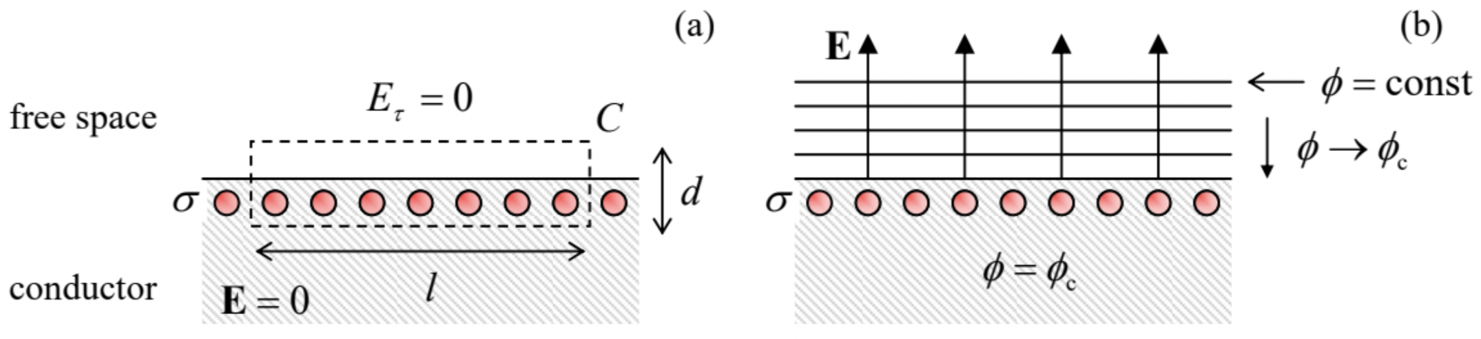 Fig. 2.2. (a) The surface charge layer at a conductor’s surface, and (b) the electric field lines and equipotential surfaces near it.
In our current case, the contour is dominated by two straight lines of length l, so that if l is much smaller than the characteristic spatial scale of field’s changes but much larger than the interatomic distances, the right-hand side of Eq. (2) may be well approximated as [(Eτ)in −(Eτ)out ]l, where Eτ is the tangential component of the corresponding macroscopic field, parallel to the surface. On the other hand, according to Eq. (1.28), the left-hand side of Eq. (2) equals zero. Hence, the macroscopic field’s component Eτ should be continuous at the surface, and to satisfy Eq. (1a) inside the conductor, the component has to vanish immediately outside it: (Eτ)out =0. This means that the electrostatic potential immediately outside of a conducting surface does not change along it. In other words, the equipotential surfaces outside a conductor should “lean” to the conductor’s surface, with their potential values
approaching the constant potential of the conductor – see Fig. 2b.
So, the electrostatic field just outside any conductor has to be normal to its surface. To find this normal field, we may use the universal relation (1.24). Since in our current case En=0 inside the conductor, we get
Surface charge density
σ=ε0(En)out ≡−ε0(∇ϕ)n≡−ε0∂ϕ∂n,
where σ is the areal density of the conductor’s surface charge. Note that deriving this universal relation between the normal component of the field and the surface charge density, we have not used any cause-vs-effect arguments, so that Eq. (3) is valid regardless of whether the surface charge is induced by an externally applied field (as in the case of conductor’s polarization, shown in Fig. 1a), or the electric field is induced by the electric charge placed on the conductor and then self-redistributed over its surface (Fig. 1b), or it is some mixture of both effects.
Before starting to use the macroscopic model for the solution of particular problems of electrostatics, let me use the balance of this section to briefly discuss its limitations. (The reader in a rush may skip this discussion and proceed to Sec. 2; however, I believe that every educated physicist has to understand when does this model work, and when it does not.)
Since the argumentation which has led to Eq. (1.24) and hence Eq. (3) is valid for any thickness d of the Gauss pillbox, within the macroscopic model, the whole surface charge is located within an infinitely thin surface layer. This is of course impossible physically: for one, this would require an infinite volumic density ρ of the charge. In reality, the charged layer (and hence the region of electric field’s crossover from the finite value (3) to zero) has a nonzero thickness λ. At least three effects contribute to λ.
(i) Atomic structure of matter. Within each atom, and frequently between the adjacent atoms as well, the genuine (“microscopic”) electric field is highly nonuniform. Thus, as was already stated above, Eq. (1) is valid only for the macroscopic field in a conductor, averaged over distances of the order of the atomic size scale a0∼10−10 m,4 and cannot be applied to the field changes on that scale. As a result, the surface layer of charges cannot be much thinner than a0.
(ii) Thermal excitation. In the conductor’s bulk, the numbers of protons of atomic nuclei (n) and electrons (ne) per unit volume are balanced, so that the net charge density, ρ=e(n−ne), vanishes.5 However, if an external electric field penetrates a conductor, free electrons can shift in or out of its affected part, depending on the field’s contribution to their potential energy, ΔU=qeϕ=−eϕ. (Here the arbitrary constant in ϕ is chosen to give ϕ=0 well inside the conductor.) In classical statistics, this change is described by the Boltzmann distribution:6
ne(r)=nexp{−U(r)kBT},
where T is the absolute temperature in kelvins (K), and kB≈1.38×10⁻²³ J/K is the Boltzmann constant. As a result, the net charge density is
ρ(r)=en(1−exp{eϕ(r)kBT}).
The penetrating electric field polarizes the atoms as well. As will be discussed in the next chapter, such polarization results in the reduction of the electric field by a material-specific dimensionless factor κ (larger, but typically not too much larger than 1), called the dielectric constant. As a result, the Poisson equation (1.41) takes the form,7
d2ϕdz2=−ρκε0=enκε0(exp{eϕkBT}−1),
where we have taken advantage of the 1D geometry of the system to simplify the Laplace operator, with the z-axis normal to the surface.
Even with this simplification, Eq. (6) is a nonlinear differential equation allowing an analytical but rather bulky solution. Since our current goal is just to estimate the field penetration depth λ, let us simplify the equation further by considering the low-field limit: e|ϕ|∼e|E|λ<<kBT. In this limit, we may extend the exponent into the Taylor series, and keep only two leading terms (of which the first one cancels with the following unity). As a result, Eq. (6) becomes linear,
d2ϕdz2=enεε0eϕkBT, i.e. d2ϕdz2=1λ2ϕ,
where the constant λ, in this case, is called the Debye screening length λD:
Debye screening length
λ2D≡κε0kBTe2n.
As the reader certainly knows, Eq. (7) describes an exponential decrease of the electric potential, with the characteristic length λD: ϕ∝exp{−z/λD}, where the z-axis is directed inside the conductor. Plugging in the fundamental constants, we get the following estimate: λD[m]≈70×(κ×T[ K]/n[ m−3])1/2. According to this formula, in semiconductors at room temperature, the Debye length may be rather substantial. For example, in silicon (κ≈12) doped to the free charge carrier concentration n=3×1018cm−3 (the value typical for modern integrated circuits),8 λD≈2 nm, still well above the atomic size scale a0. In this case, Eq. (8) should not be taken literally, because it is based on the assumption of a continuous charge distribution.
(iii) Quantum statistics. Actually, the last estimate is not valid for good metals (and highly doped semiconductors) for one more reason: their free electrons obey the quantum (Fermi-Dirac) statistics rather than the Boltzmann distribution (4).9 As a result, at all realistic temperatures the electrons form a degenerate quantum gas, occupying all available energy states below certain energy level EF≫kBT, called the Fermi energy. In these conditions, the screening of relatively low electric field may be described by replacing Eq. (5) with
ρ=e(n−ne)=eg(EF)(−U)=−e2g(EF)ϕ,
where g(E) is the density of quantum states (per unit volume per unit energy) at electron’s energy E. At the Fermi surface, the density is of the order of n/EF.10 As a result, we again get the second of Eqs. (7), but with a different characteristic scale λ, defined by the following relation:
Thomas-Fermi screening length
λ2TF≡κε0e2g(EF)∼κε0EFe2n,
and called the Thomas-Fermi screening length. Since for most good metals, n is of the order of 1029 m−3, and EF is of the order of 10 eV, Eq. (10) typically gives λTF close to a few a0, and makes the Thomas-Fermi screening theory valid at least semi-quantitatively.
To summarize, the electric field penetration into good conductors is limited to a depth λ ranging from a fraction of a nanometer to a few nanometers, so that for problems with the characteristic size much larger than that scale, the macroscopic model (1) gives very good accuracy, and we will use them in the rest of this chapter. However, the reader should remember that in many situations involving semiconductors, as well as at some nanoscale experiments with metals, the electric field penetration should be taken into account.
Another important condition of the macroscopic model’s validity is imposed on the electric field’s magnitude, which is especially significant for semiconductors. Indeed, as Eq. (6) shows, Eq. (7) is only valid if e|ϕ|<<kBT, so that |E|∼|ϕ|/λD should be much lower than kBT/eλD. In the example given above (λD≈2 nm,T=300 K), this means |E|<<Et∼107 V/m≡105 V/cm - the value readily reachable in the lab. At larger fields, the field penetration becomes nonlinear, leading in particular to the very important effect of carrier depletion; it will be discussed in SM Sec. 6.4. For typical metals, such linearity limit, Et∼EF/eλTF is much higher, ∼1011 V/m, but the model may be violated at lower fields by
other effects, such as the impact-ionization leading to electric breakdown, which may start at ∼107 V/m.
Reference
1 A more detailed discussion of the electrostatic field screening may be found, e.g., in SM Sec. 6.4. (Alternatively, see either Sec. 13.5 of J. Hook and H. Hall, Solid State Physics, 2nd ed., Wiley, 1991; or Chapter 17 of N. Ashcroft and N. Mermin, Solid State Physics, Brooks Cole, 1976.)
2 This term, used for the electric field, should not be confused with shielding – the word used for the description of the magnetic field reduction by magnetic materials – see Chapter 5 below.
3 See, e.g., MA Eq. (12.1).
4 This scale originates from the quantum-mechanical effects of electron motion, characterized by the Bohr radius rB≡ℏ2/me(e2/4πε0)≈0.53×10−10 m – see, e.g., QM Eq. (1.10). It also defines the scale EB=e/4πε0r2B∼1012 SI units (V/m) of the microscopic electric fields inside the atoms. (Please note how large these fields are.)
5 In this series, e denotes the fundamental charge, e≈1.6×10⁻¹⁹ C>0, so that the electron’s charge equals (−e).
6 See, e.g., SM Sec. 3.1.
7 This equation and/or its straightforward generalization to the case of charged particles (ions) of several kinds is frequently (especially in the theories of electrolytes and plasmas) called the Debye-Hückel equation.
8 There is a good reason for making an estimate of λD for this case: the electric field created by the gate electrode of a field-effect transistor, penetrating into doped silicon by a depth ∼λD, controls the electric current in this most important electronic device – on whose back all our information technology rides. Because of that, λD establishes the possible scale of semiconductor circuit shrinking, which is the basis of the well known Moore’s Law. (Practically, the scale is determined by integrated circuit patterning techniques, and Eq. (8) may be used to find the proper charge carrier density n and hence the necessary level of silicon doping – see, e.g., SM Sec. 6.4.)
9 See, e.g., SM Sec. 2.8. For a more detailed derivation of Eq. (10), see SM Chapter 3.
10 See, e.g., SM Sec. 3.3.